
Method for line density multiplication using block copolymers and sequential infiltration synthesis

a technology of block copolymer and density multiplication, applied in the field of nanotechnology, can solve the problems of degraded etched substrates, deformation of etched substrates, and tilted sidewall spacers

Active Publication Date: 2015-08-13
WESTERN DIGITAL TECH INC
View PDF1 Cites 318 Cited by
  • Summary
  • Abstract
  • Description
  • Claims
  • Application Information

AI Technical Summary

Benefits of technology

This patent describes a method for making a patterned substrate using a special polymer called block copolymers (BCPs) and atomic layer deposition (ALD). The BCPs are deposited on the substrate and annealed to form parallel stripes with a pattern of interfaces between them. The interfaces contain a reactive functional group that reacts with the ALD precursors, resulting in the infiltration of inorganic material without affecting the BCP components. The BCP components and functional groups are then removed, leaving a pattern of parallel lines of inorganic material with a smaller pitch than the original BCP components. The inorganic lines can then be used as an etch mask to etch the underlying substrate, which can then be used as a nanoimprint template. The invention allows for a halving of the pitch and a doubling of the line density on a substrate.

Problems solved by technology

Current photolithography has reached fundamental printing limits.
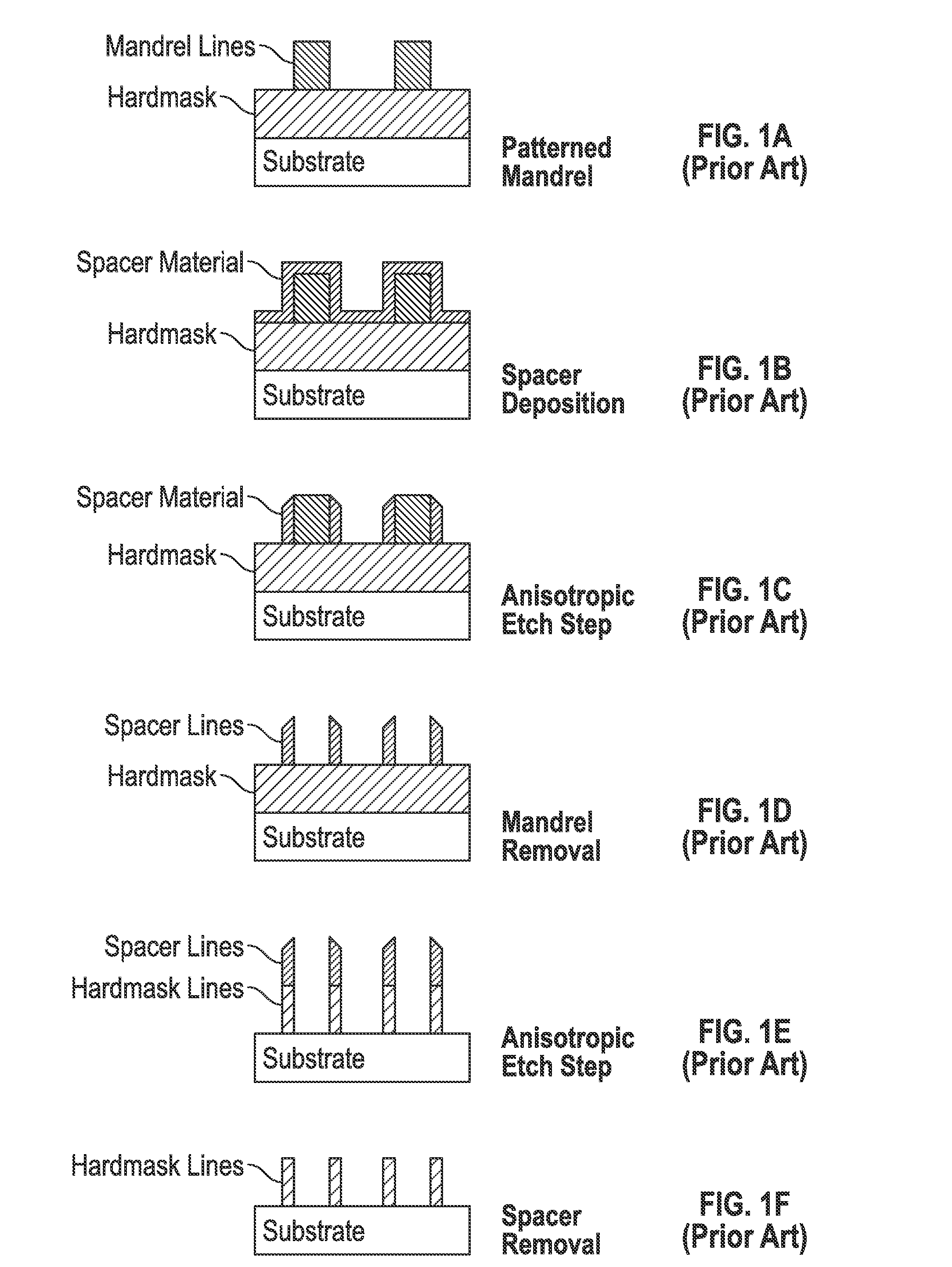
A problem with the prior art method of line density multiplication by the use of sidewall spacers is that the sidewall spacers formed on the mandrel stripes are used as the final etch mask to etch the substrate.
However, the mandrel stripes are often not precisely perpendicular to the substrate, resulting in tilted sidewall spacers and degraded etched substrates.

Method used


Image

  • Method for line density multiplication using block copolymers and sequential infiltration synthesis
  • Method for line density multiplication using block copolymers and sequential infiltration synthesis
  • Method for line density multiplication using block copolymers and sequential infiltration synthesis

Examples


Embodiment Construction

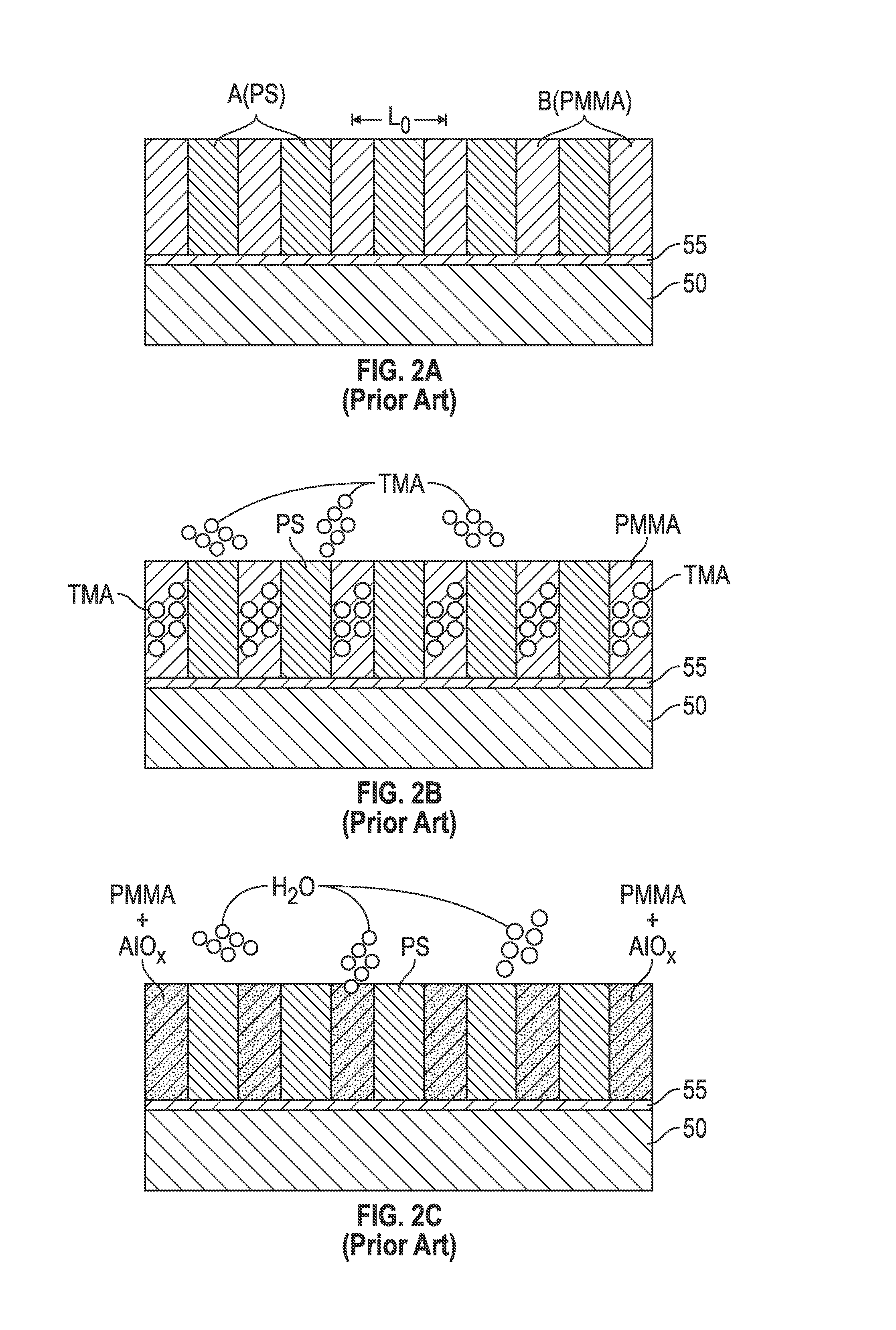
[0013]Self-assembling block copolymers (BCPs) have been proposed for creating periodic nanometer (nm) scale features. Self-assembling BCPs typically contain two or more different polymeric block components, for example components A and B, that are immiscible with one another. Under suitable conditions, the two or more immiscible polymeric block components separate into two or more different phases or microdomains on a nanometer scale and thereby form ordered patterns of isolated nano-sized structural units. There are many types of BCPs that can be used for forming the self-assembled periodic patterns. If one of the components A or B is selectively removable without having to remove the other, then an orderly arranged structural units of the un-removed component can be formed.

[0014]Specific examples of suitable BCPs that can be used for forming the self-assembled periodic patterns include, but are not limited to: poly(styrene-block-methyl methacrylate) (PS-b-PMMA), poly(ethylene oxid...


PUM

PropertyMeasurementUnit
Structureaaaaaaaaaa

Abstract

Block copolymers (BCPs) and synthetic infiltration synthesis (SIS) are used to double the line density on a substrate. The BCP comprises first and second interconnected BCP components with a functional group at the junction or interface of the components. After deposition of the BCP on the substrate and annealing, a pattern of parallel stripes of first and second BCP components is formed with a pattern of functional group interfaces between the components. Each of the BCP components is non-reactive with atomic layer deposition (ALD) precursors, while the functional group is reactive with the ALD precursors. The ALD results in the infiltration of inorganic material into the interfaces where the reactive functional groups are located but without affecting the BCP components. After removal of the organic material, a pattern of parallel lines of inorganic material remains with a pitch half that of the stripes of BCP components.

Description

BACKGROUND OF THE INVENTION[0001]1. Field of the Invention[0002]This invention relates to line density multiplication in the area of nanotechnology, such as the fabrication of semiconductor devices and nanoimprint templates.[0003]2. Description of the Related Art[0004]Current photolithography has reached fundamental printing limits. As a result, it is necessary to develop processes for line density multiplication. One process that is gaining recognition for use in DRAM and NAND flash manufacturing is sidewall spacer “line doubling”, sometimes also referred to as “line multiplication”, “frequency doubling”, “self-aligned double patterning (SADP)”, “sidewall image transfer” or “pitch-halving”. The process also has application in making imprint templates, which may be used for making bit-patterned-media (BPM) magnetic recording disks. For example, U.S. Pat. No. 7,758,981 B2, which is assigned to the same assignee as this application, describes a method using sidewall spacer line doubli...

Claims


Application Information

Patent Timeline
IPC IPC(8): C23C16/455C23C16/40C23C16/22
CPCC23C16/45525C23C16/22C23C16/402C23C16/407C23C16/403C23C16/401C23C16/405G03F7/0002H01L21/0271H01L21/0335H01L21/3083
Inventor ARORA, HITESHRUIZ, RICARDO
Owner WESTERN DIGITAL TECH INC
Learn More