Array Substrate and Liquid Crystal Display Device

Active Publication Date: 2015-08-20
BOE TECH GRP CO LTD
View PDF4 Cites 8 Cited by
  • Summary
  • Abstract
  • Description
  • Claims
  • Application Information

AI Technical Summary

Benefits of technology

[0007]To solve the problem of low transmissivity of the conventional FFS mode or ADS mode liquid c

Problems solved by technology

The electric field at the edges of the slit electrode is easily disturbed, and has poor driving capability for the liquid crystal molecules, which results in a low efficiency of th

Method used


Image

  • Array Substrate and Liquid Crystal Display Device
  • Array Substrate and Liquid Crystal Display Device
  • Array Substrate and Liquid Crystal Display Device

Examples


embodiment 1

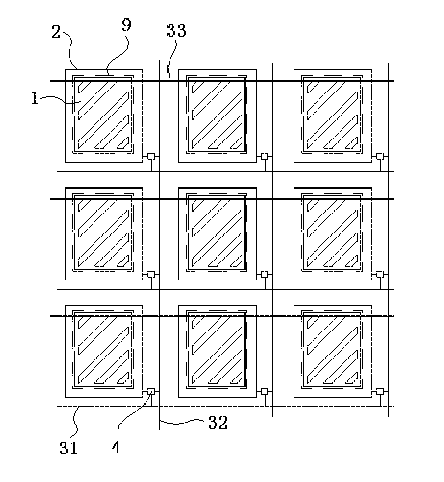
[0031]As shown in FIG. 2, the present embodiment provides an array substrate comprising intersecting gate lines 31 and data lines 32 which are intersected each other. A TFT 4 is provided at each of the intersections of the gate lines 31 and data lines 32, and a pixel unit 9 is defined for displaying necessary contents independently.

[0032]The array substrate is of FFS mode or ADS mode. Each pixel unit 9 is provided with a plate electrode 2 and a slit electrode 1 arranged above the plate electrode 2. An insulation layer (not shown) is arranged between the plate electrode 2 and the slit electrode 1.

[0033]As shown in FIG. 2, the plate electrode 2 in each pixel unit 9 extends to the peripheral region of the pixel unit 9, i.e., the plate electrode 2 exceeds the boundary of the pixel unit 9. The slit electrode 1 also extends to the peripheral region of the pixel unit 9, the plate electrode 2 and the slit electrode 1 are provided simultaneously in at least part of the peripheral region of t...

embodiment 2

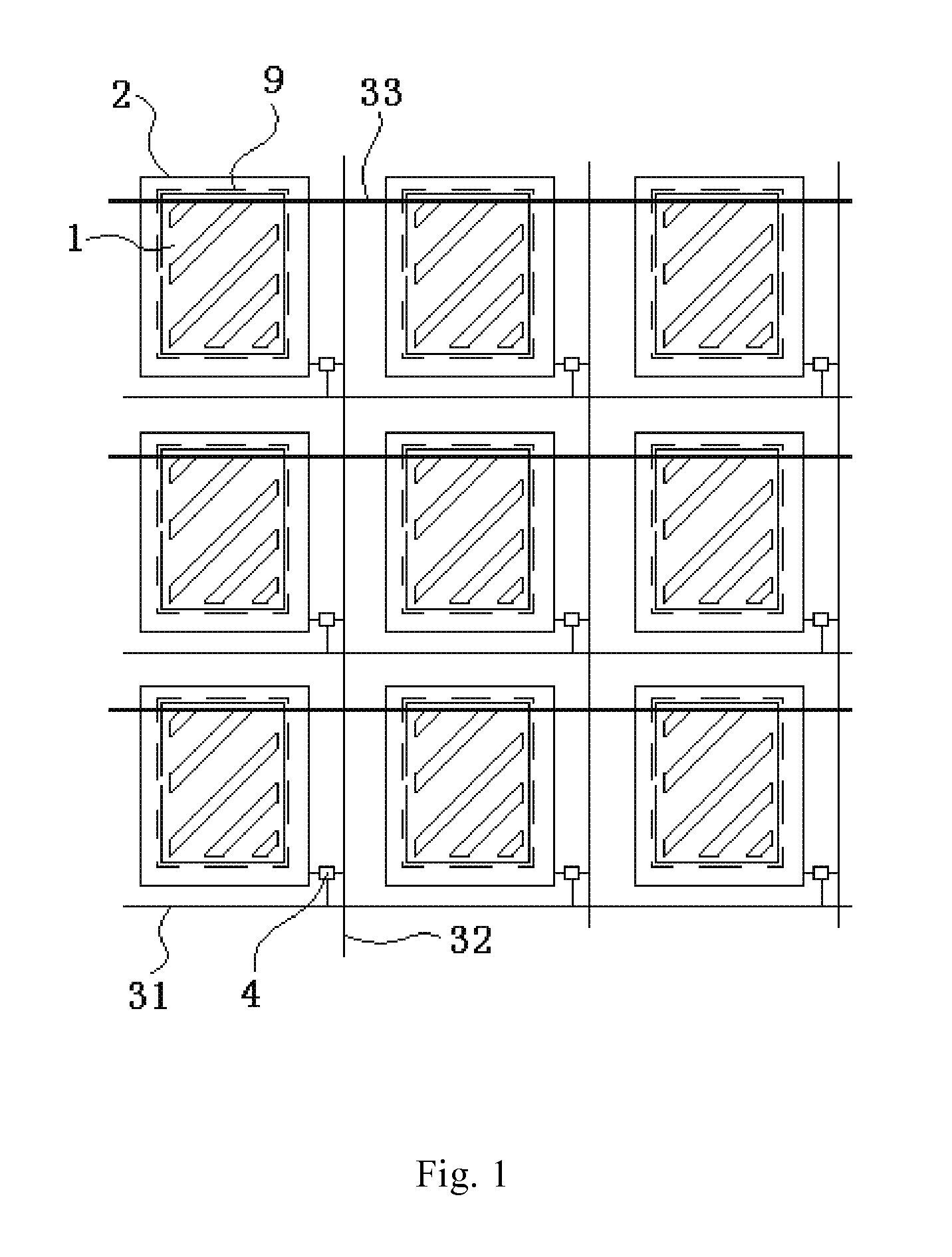
[0042]As shown in FIG. 3, the present embodiment provides an array substrate having a similar structure to that in the Embodiment 1.

[0043]The difference therebetween is that the array substrate according to the present embodiment utilizes a “dual gate lines” design, wherein the number of the gate lines 31 is doubled and that of the data lines 32 is halved, such design can reduce the number of the Data Driver ICs and the costs.

[0044]Specifically, as shown in FIG. 3, the disposing direction of the gate lines 31 is set as the row direction, and the disposing direction of the data lines 32 is set as the column direction. Two gate lines 31 are provided between two adjacent rows of pixel units 9, and every two pixel units 9 among the row of pixel units 9 are alternatively connected to two gate lines 31 at both sides of the row of pixel units 9. A data line 32 is provided at intervals of two columns of pixel units 9, each data line 32 is connected with two columns of pixel units 9 at both ...

embodiment 3

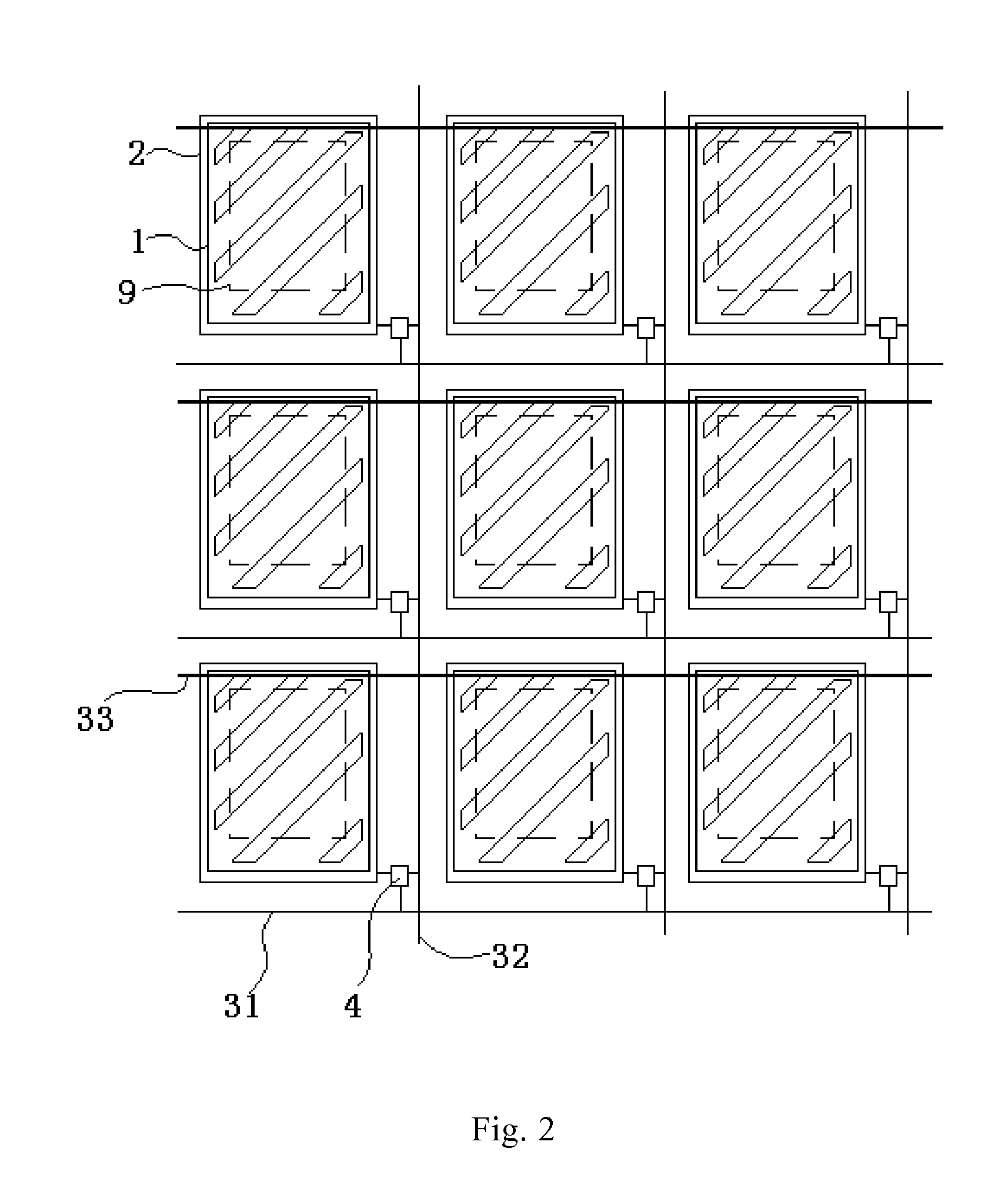
[0053]As shown in FIG. 4, the present embodiment provides an array substrate having a similar structure to that in the Embodiment 2.

[0054]The difference therebetween is that the present embodiment uses a “dual data lines” design instead of the “dual gate lines” design.

[0055]As shown in FIG. 4, in the array substrate of the present embodiment, the number of the data lines 32 is doubled and that of the gate lines 31 is halved. Specifically, the disposing direction of the gate lines 31 is set as the row direction, and the disposing direction of the data lines 32 is set as the column direction. A gate line 31 is provided at intervals of 2 rows of pixel units 9, each gate line 31 is connected with 2 rows of pixel units 9 at both sides of the gate line 31 simultaneously. Two data lines 32 are provided between two adjacent columns of pixel units 9, and every two pixel units 9 among each column of pixel units 9 are alternatively connected to two data lines 32 at both sides of the column of ...


PUM


Abstract

The present invention relates to the field of liquid crystal display technology and provides an array substrate and a liquid crystal display device which can solve the problem of low transmissivity of existing liquid crystal display devices. The array substrate of the present invention comprises a plurality of pixel units, each pixel unit is provided with a plate electrode and a slit electrode arranged above the plate electrode, an insulation layer is provided between the plate electrode and the slit electrode, and the plate electrode extends to the periphery region of the pixel unit, the slit electrode extends to the periphery region of the pixel unit; the slit electrode and the plate electrode are both provided in at least part of the peripheral region of the pixel unit. the present invention is applicable to liquid crystal display devices, especially the liquid crystal display devices taking a “dual gate lines” design.

Description

FIELD OF THE INVENTION[0001]The present invention relates to the field of liquid crystal display technology, in particular to an array substrate and a liquid crystal display device.BACKGROUND OF THE INVENTION[0002]FFS (Fringe Field Switching) or ADS (Advanced Dimension Switch) mode liquid crystal display device is becoming a research hotspot in development of the liquid crystal display device for the advantages of high transmissivity, wide viewing angle, wide color gamut and so on.[0003]As shown in FIG. 1, a plurality of pixel units 9 for display (i.e. for outputting light) are arranged on the array substrate of the FFS mode or ADS mode liquid crystal display device, each pixel unit 9 is provided with a plate electrode 2, a slit electrode 1 is provided above the plate electrode 2, and an insulation layer (not shown) is provided between the plate electrode 2 and the slit electrode 1. The regions between the pixel units 9 (i.e., the peripheral region of the pixel units 9) are used for...

Claims


Application Information

Patent Timeline
IPC IPC(8): H01L27/12G02F1/1362G02F1/1333G02F1/1368G02F1/1343
CPCH01L27/124G02F1/1368G02F1/136286G02F1/133345G02F1/13439G02F1/134363G02F2201/40G02F1/134372
Inventor PENG, KUANJUNTIAN, YUNYUNCHOI, HYUNSICKIM, HEECHEOL
Owner BOE TECH GRP CO LTD
Why Eureka
Try Eureka