Organic electroluminescent element and electronic instrument
Active Publication Date: 2015-08-20
IDEMITSU KOSAN CO LTD
View PDF3 Cites 19 Cited by
Summary
Abstract
Description
Claims
Application Information
AI Technical Summary
This helps you quickly interpret patents by identifying the three key elements:
Problems solved by technology
Method used
Benefits of technology
Benefits of technology
The patent text aims to provide an organic electroluminescence device that can reduce the directionality of radiation light and improve external quantum efficiency. This would make it easier to create more efficient and effective electronic equipment using this technology.
Problems solved by technology
However, the adjustment of the optical interference distance is not sufficient for extracting light trapped within the device.
It is considered to be the most difficult to extract the light in the surface plasmon mode as compared with the other optical modes.
Method used
Image
Click on the blue label to locate the original text in one second.
Reading with bidirectional positioning of images and text.
Examples
first exemplary embodiment
Advantages of First Exemplary Embodiment
[0094]According to the first exemplary embodiment as described above, the following advantages can be obtained.
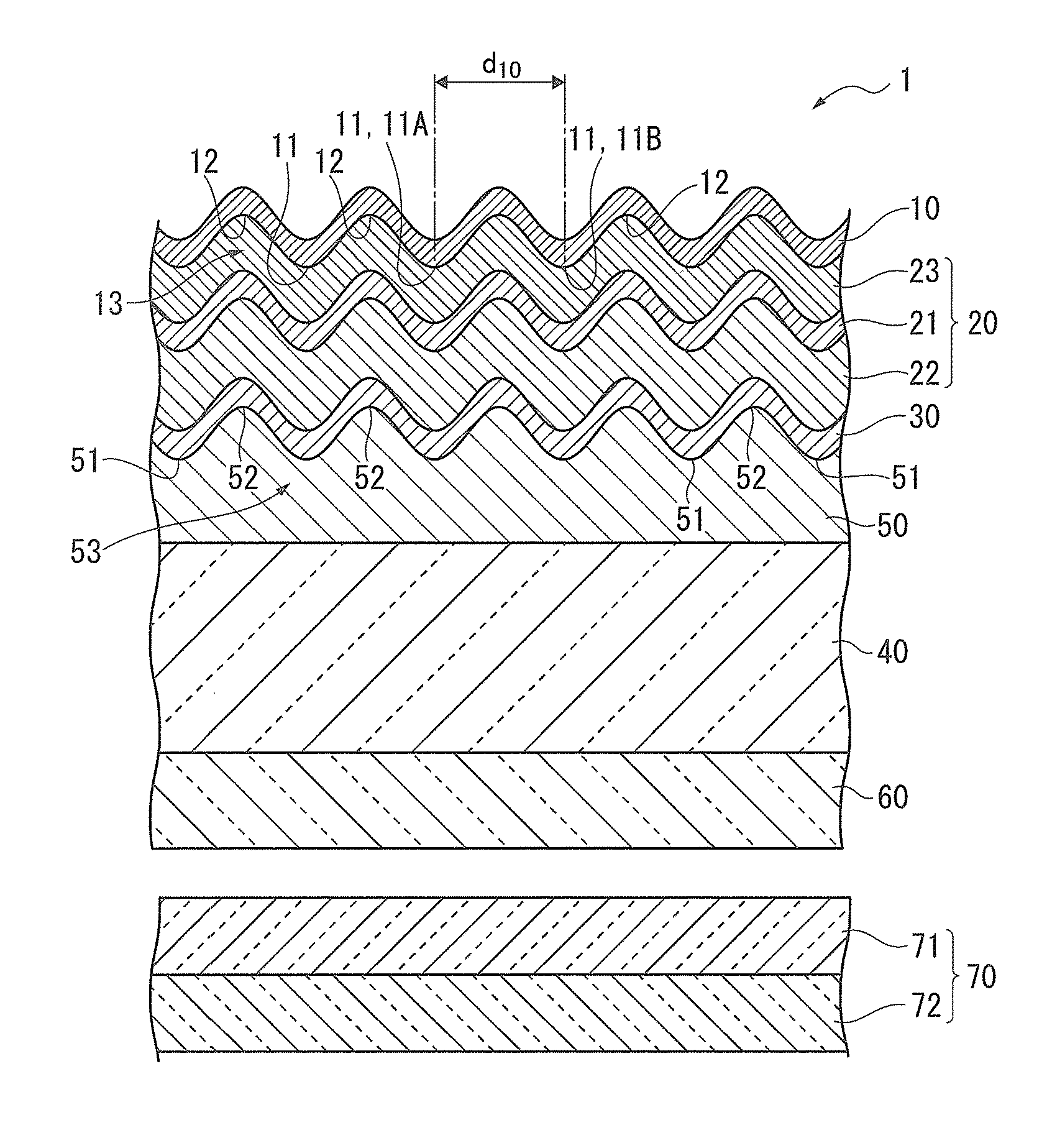
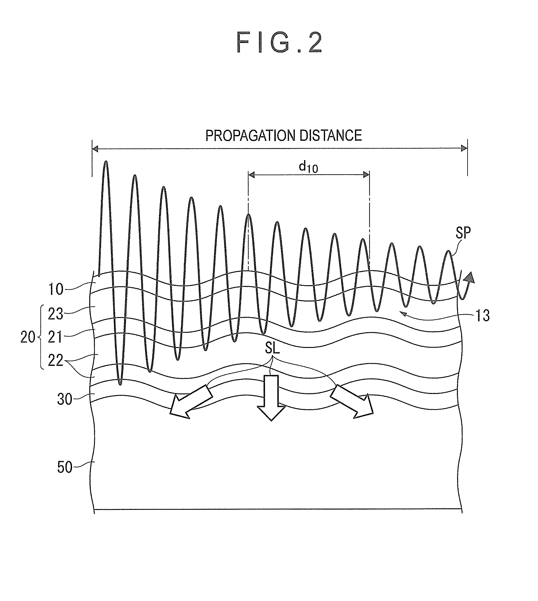
[0095]In the organic EL device 1, the first electrode 10 has the second convexo-concave structure 13 at the interface with the second organic layer 23. The second convexo-concave structure 13 is shaped in a sine-wave curve or a curve represented by a sum of a plurality of sine waves having different amplitudes or angles. The second-convex-portion distance d10 of the second convexo-concave structure 13 is equal to or more than the peak wavelength of the light radiated from the emitting layer 21 and is equal to or less than the propagation distance (Lsp) of the surface plasmon at the interface between the first electrode 10 and the second organic layer 23.
[0096]According to the organic EL device 1 having the above arrangement, the light in the surface plasmon mode propagated in the in-plane direction of the organic EL device 1 is scatte...
second exemplary embodiment
[0101]Next, a second exemplary embodiment of the invention will be described.
[0102]In the description of the second exemplary embodiment, the same components as those in the first exemplary embodiment are denoted by the same reference signs and names to simplify or omit an explanation of the components. In the second exemplary embodiment, the same materials and compounds as described in the first exemplary embodiment are usable.
[0103]In the organic EL device 1 of the first exemplary embodiment, both of the first electrode 10 and the second electrode 30 have the above convexo-concave structure. However, in an organic EL device of the second exemplary embodiment, either one of the first electrode 10 and the second electrode 30 may have a convexo-concave structure.
[0104]In this arrangement, it is preferable that an electrode (the first electrode 10 in the second exemplary embodiment) in an opposite direction from an extraction direction of the light radiated from the emitting layer 21 ...
embodiment (
Modifications of Embodiment(s)
[0109]It should be noted that the invention is not limited to the above exemplary embodiment but may include any modification and improvement as long as such modification and improvement are compatible with the invention.
[0110]In the above exemplary embodiments, the organic EL device having the outer-light extraction layer 60 is described as an example, but the arrangement of the organic EL device is not limited thereto. For instance, the optical member 70 may be provided to an opposite surface of the light-transmissive substrate 40 from a surface thereof facing the inner-light extraction layer 50 without the outer-light extraction layer 60.
[0111]Moreover, in the above exemplary embodiments, the organic EL device having the optical member 70 is described as an example, but the arrangement of the organic EL device is not limited thereto. For instance, only the outer-light extraction layer 60 may be provided on the opposite surface of the light-transmissi...
PUM
Abstract
The first electrode has a convexo-concave structure including a plurality of convex portions and a plurality of concave portions at an interface with the organic compound layer. The convexo-concave structure has at least one cross section in a thickness direction of the light-transmissive substrate, the cross section being shaped in a sine-wave curve or a curve represented by a sum of a plurality of sine waves having different amplitudes or angles. A distance between a convex portion and an adjacent convex portion forming the convexo-concave structure is equal to or more than a peak wavelength of light radiated from the emitting layer and is equal to or less than a propagation distance (Lsp) of surface plasmon at the interface between the first electrode having the convexo-concave structure and the organic compound layer.
Description
TECHNICAL FIELD[0001]The present invention relates to an organic electroluminescence device and electronic equipment provided with the organic electroluminescence device.BACKGROUND ART[0002]There has been known an organic electroluminescence device (hereinafter, occasionally referred to as an “organic EL device”) that includes an organic compound layer (in which an emitting layer is included) between an anode and a cathode and emits light using exciton energy generated in the organic compound layer by a recombination of holes injected into the emitting layer from the anode and electrons injected into the emitting layer from the cathode.[0003]Such an organic EL device, which has the advantages as a self-emitting device, is expected to serve as an emitting device excellent in luminous efficiency, image quality, power consumption and thin design.[0004]In an optical design of the organic EL device, adjustment of an optical interference distance and the like are conducted in order to imp...
Claims
Application Information
Patent Timeline
Application Date:The date an application was filed.
Publication Date:The date a patent or application was officially published.
First Publication Date:The earliest publication date of a patent with the same application number.
Issue Date:Publication date of the patent grant document.
PCT Entry Date:The Entry date of PCT National Phase.
Estimated Expiry Date:The statutory expiry date of a patent right according to the Patent Law, and it is the longest term of protection that the patent right can achieve without the termination of the patent right due to other reasons(Term extension factor has been taken into account ).
Invalid Date:Actual expiry date is based on effective date or publication date of legal transaction data of invalid patent.

