

Semiconductor structure and method for manufacturing the same
a technology of semiconductor devices and structure, applied in the direction of semiconductor devices, electrical equipment, transistors, etc., can solve the problems of increasing the difficulty of implementing such a gate line patterning process, the lithography process is facing greater demands and challenges, and the extremely precise distance becomes increasingly difficult to achieve. achieve the effect of facilitating the subsequent process and ensuring the performance of semiconductor devices
- Summary
- Abstract
- Description
- Claims
- Application Information
AI Technical Summary
Benefits of technology
Problems solved by technology
Method used
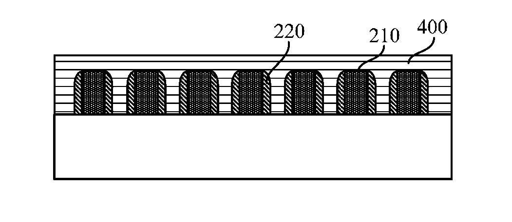
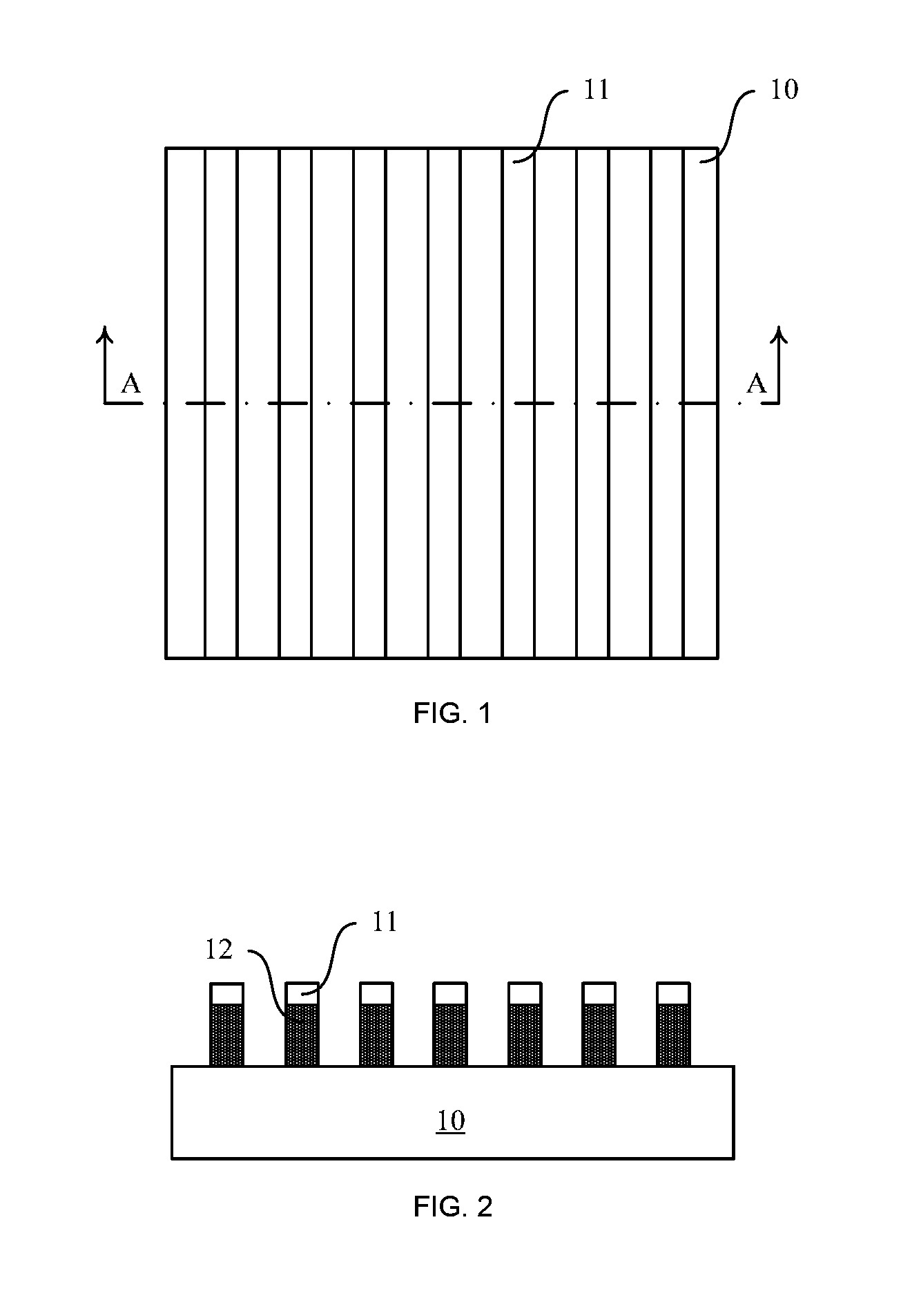
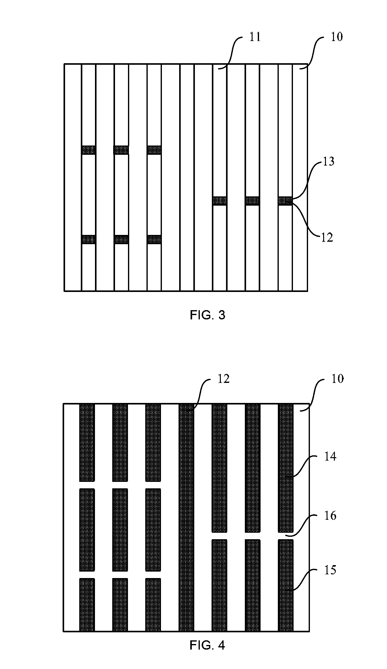
Image

Examples
Embodiment Construction
[0025]The objectives, technical solutions and advantages of the present invention are made more evident according to the following detailed description of exemplary embodiments in conjunction with the accompanying drawings.
[0026]Embodiments of the present invention will be described in detail below, wherein examples of embodiments are illustrated in the appended drawings, in which same or similar reference signs throughout denote same or similar elements, or elements having same or similar functions. It should be understood that embodiments described below in conjunction with the drawings are illustrative. These embodiments are provided for explaining the present invention only, and thus shall not be interpreted as a limit to the present invention.
[0027]Various embodiments or examples are provided here below to implement different structures of the present invention. To simplify the disclosure of the present invention, descriptions of components and arrangements of specific examples...
PUM
 Abstract
Description
Claims
Application Information