Semiconductor device manufacturing apparatus

a manufacturing apparatus and semiconductor technology, applied in lighting and heating apparatus, muffle furnaces, furnaces, etc., can solve the problems of reducing the efficiency of semiconductor device manufacturing, increasing the vertical size of storage containers, and unable to efficiently perform heat treatment on sic substrates

Active Publication Date: 2015-09-03
TOYO TANSO KK
View PDF15 Cites 8 Cited by
  • Summary
  • Abstract
  • Description
  • Claims
  • Application Information

AI Technical Summary

Benefits of technology

[0027]Accordingly, an apparatus for manufacturing a semiconductor device, that can exert the above-described effects, is achieved.

Problems solved by technology

As a result, the heat treatment on a SiC substrate cannot be efficiently performed, which leads to reduction in the efficiency of semiconductor device manufacture.
This leads to an increase in the vertical size of the storage container.

Method used


Image

  • Semiconductor device manufacturing apparatus
  • Semiconductor device manufacturing apparatus
  • Semiconductor device manufacturing apparatus

Examples


Embodiment Construction

[0039]Next, an embodiment of the present invention will be described with reference to the drawings.

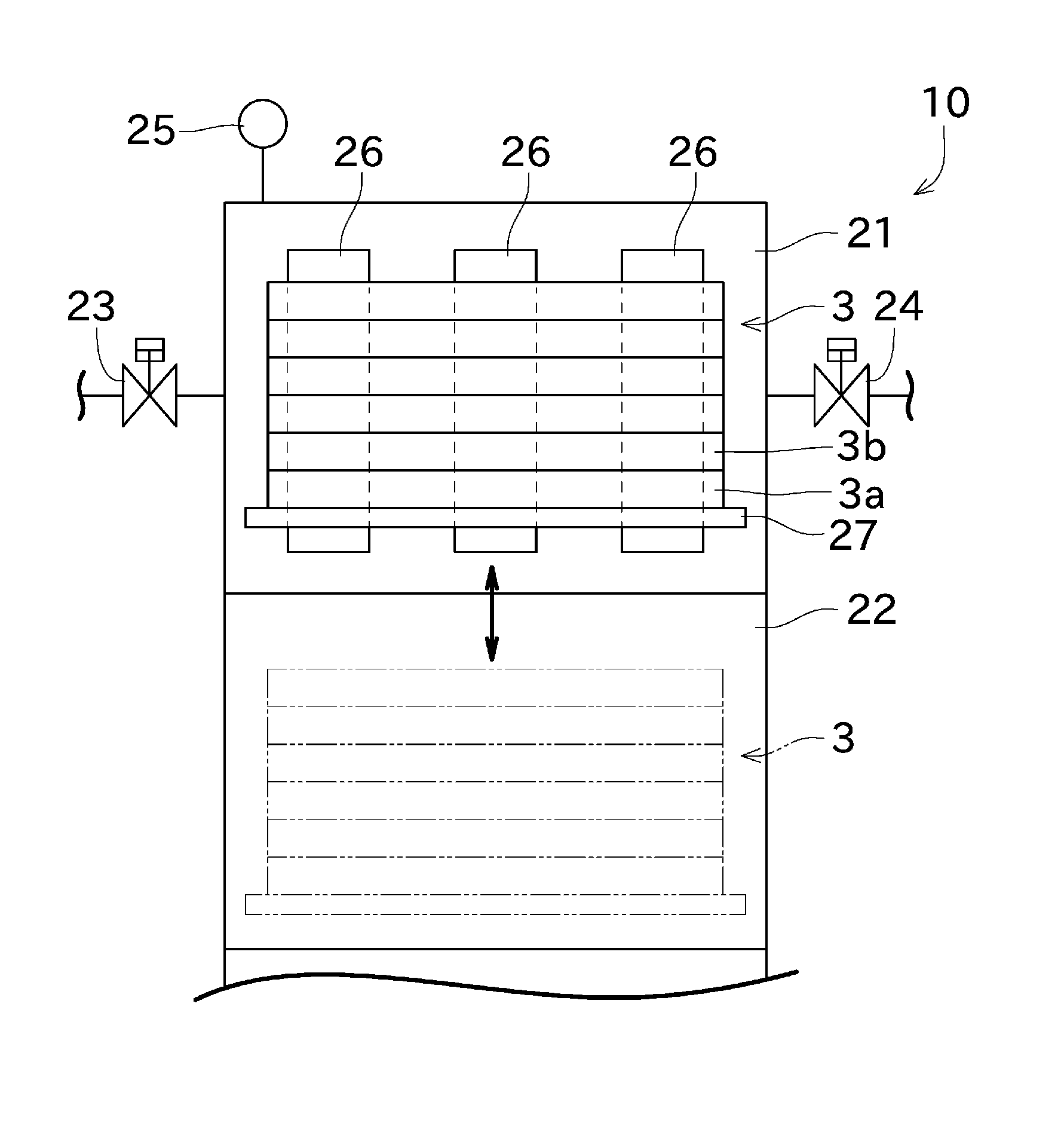
[0040]Firstly, referring to FIG. 1, a high temperature vacuum furnace (apparatus for manufacturing a semiconductor device) 10 used for a heat treatment of this embodiment will be described. FIG. 1 is a diagram illustrating outline of a high temperature vacuum furnace used for a surface treatment method of the present invention.

[0041]As shown in FIG. 1, the high temperature vacuum furnace 10 includes a main heating chamber 21 and a preheating chamber 22. The main heating chamber 21 is configured to heat a SiC substrate made of, at least in its surface, single crystal SiC, up to a temperature of 1000° C. or more and 2300° C. or less. The preheating chamber 22 is a space for preheating a SiC substrate prior to heating of the SiC substrate in the main heating chamber 21.

[0042]A vacuum-forming valve 23, an inert gas injection valve 24, and a vacuum gauge 25 are connected to the main heatin...


PUM

PropertyMeasurementUnit
temperatureaaaaaaaaaa

Abstract

Provided is a heat treatment container having a small size and capable of efficiently performing a heat treatment on a SiC substrate. A heat treatment container is a container for a heat treatment on a SiC substrate 40 under Si vapor pressure. The SiC substrate 40 is made of, at least in a surface thereof, single crystal SiC. The heat treatment container includes a container part 30 and a substrate holder 50. The container part 30 includes an internal space 33 in which Si vapor pressure is caused. The internal space 33 is partially open. The substrate holder 50 is able to support the SiC substrate 40. When the substrate holder 50 supports the SiC substrate 40, an open portion of the container part 30 is covered so that the internal space 33 is hermetically sealed.

Description

BACKGROUND OF THE INVENTION[0001]1. Field of the Invention[0002]The present invention relates mainly to a heat treatment container in which a SiC substrate is heated under Si vapor pressure for etching.[0003]2. Description of the Related Art[0004]SiC, which is superior to Si or the like in, for example, heat resistance and electrical characteristics, has attracted attention as a new semiconductor material.[0005]Japanese Patent Application Laid-Open No. 2008-16691 discloses a surface treatment method for planarizing a surface of a SiC substrate. In the surface treatment method, a SiC substrate is heat-treated while being stored in a storage container (heat treatment container). The storage container includes an upper container and a lower container that are fittable to each other. The storage container, when the upper container and the lower container are fitted to each other, forms a hermetically sealed space. A heat treatment is performed with the upper container and the lower cont...

Claims


Application Information

Patent Timeline
Patent Type & Authority Applications(United States)
IPC IPC(8): H01L21/67F27D11/00F27D7/06
CPCH01L21/67098H01L21/67069F27D2007/063F27D11/00F27D7/06H01L21/67109H01L21/67346H01L21/67386F27B17/0025F27D5/0037F27D11/02F27D2005/0081
Inventor TORIMI, SATOSHIYABUKI, NORIHITONOGAMI, SATORU
Owner TOYO TANSO KK
Why Eureka
Try Eureka