Sensing circuit structure and manufacturing method of same

Inactive Publication Date: 2015-10-01
J TECH MATERIAL
View PDF6 Cites 4 Cited by
  • Summary
  • Abstract
  • Description
  • Claims
  • Application Information

AI Technical Summary

Benefits of technology

[0007]The present invention has been accomplished under the circumstances in view. It is the main object of the present invention to provide a sensing circuit structure and its manufacturing method, which red

Problems solved by technology

Further, the formation of the surface treatment layer as described above is c

Method used


Image

  • Sensing circuit structure and manufacturing method of same
  • Sensing circuit structure and manufacturing method of same
  • Sensing circuit structure and manufacturing method of same

Examples


Embodiment Construction

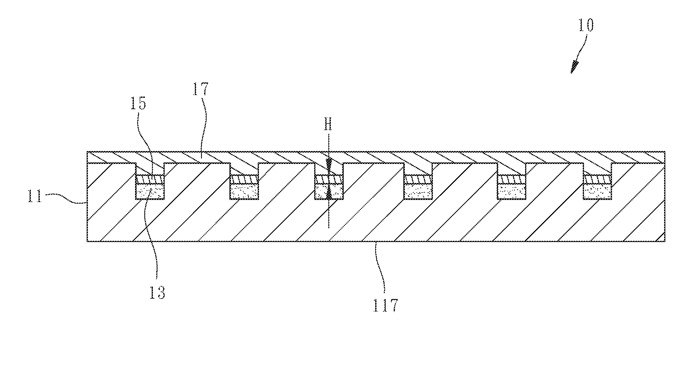
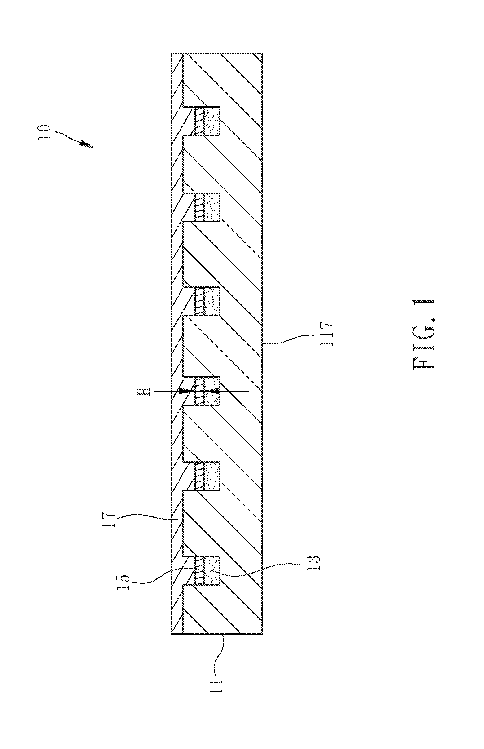
[0019]Referring to FIG. 1, a sensing circuit structure in accordance with the present invention is adapted for use in a projected capacitive touch panel, in which the human eye is difficult to observe directly the circuit pattern (metal mesh) of the sensing circuit structure when the touch panel is being flipped. The composition of the sensing circuit structure and its manufacturing method will be described hereinafter in details.

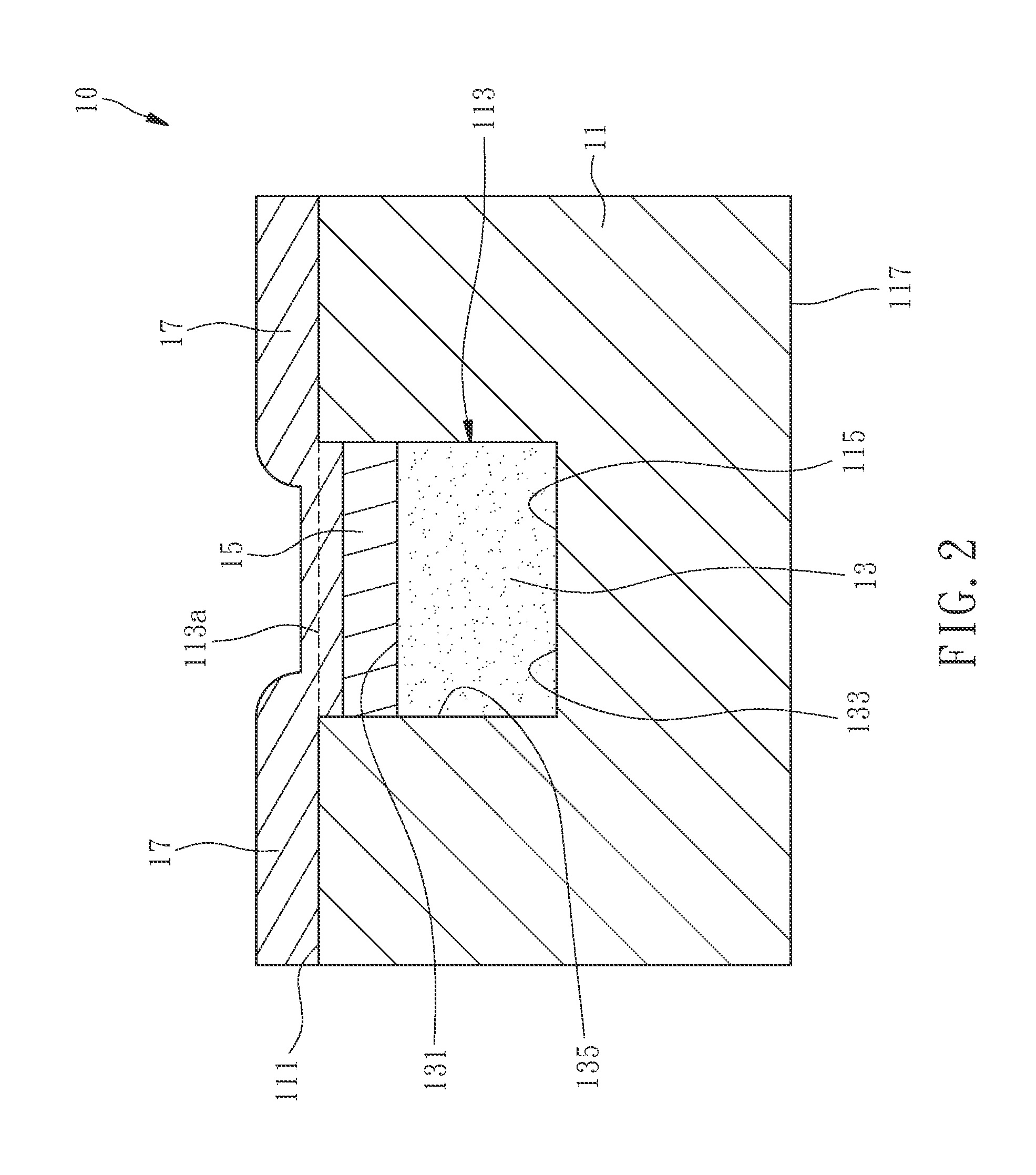
[0020]Referring to FIGS. 1 and 2, the sensing circuit structure 10 of the present invention comprises a transparent substrate 11, a plurality of plating base layers 13 and a plurality of metal conductor layers 15.

[0021]The transparent substrate 11 comprises a plurality of grooves 113 located in a surface 111 thereof. Further, the transparent substrate 11 has a first refractive index in visible light and a first visible light transmittance.

[0022]The plating base layers 13 are respectively connected to the transparent substrate 11 and respectively located in ...


PUM

PropertyMeasurementUnit
Thicknessaaaaaaaaaa
Thicknessaaaaaaaaaa
Coloraaaaaaaaaa

Abstract

A method for making a sensing circuit structure is disclosed to provide a transparent substrate, and then to form multiple plating base layers in the transparent substrate in a spaced manner, and then to form a metal conductor layer on each plating base layer using a plating technique. Thus, the thickness of the metal conductor layers can be thinner than that formed by silver paste. The invention relates also to a sensing circuit structure made by this method.

Description

BACKGROUND OF THE INVENTION[0001]1. Field of the Invention[0002]The present invention relates to sensing circuit technology for touch panel and more particularly, to a sensing circuit structure and its manufacturing method.[0003]2. Description of the Related Art[0004]US Patent 20120327021 discloses a capacitive touch panel and a method for manufacturing the same. This patent discloses a sensing layer manufacturing process. This manufacturing process is substantially as follows: Employ a surface treatment process to the surface of the inner surface of the recessed transparent substrate and the resin layer, thereby forming a surface treatment layer. The surface treatment process can be a chemical etching process using an alkaline aqueous solution or catalyst, a plasma surface treatment process, or an ion beam surface treatment process. Thereafter, form a metallic seed layer on the surface treatment layer. Actually, the surface treatment layer is a resin layer for the deposition of the...

Claims


Application Information

Patent Timeline
IPC IPC(8): G06F3/044H05K3/46H05K3/04G06F1/16
CPCG06F3/044G06F1/16H05K3/4673G06F2203/04103H05K3/4664H05K3/04G06F2203/04112H05K3/4661H05K3/0014H05K3/107H05K3/182H05K3/22H05K3/244H05K2201/0108H05K2201/0329H05K2201/09118H05K2203/0315H05K2203/0545H05K2203/0709
Inventor HSU, PO-YICHIU, CHENG-WEI
Owner J TECH MATERIAL
Why Eureka
Try Eureka