Method and system for a low-loss optical y-junction power splitter

a power splitter and optical y-junction technology, applied in the field of semiconductor photonics, can solve the problems of cable bulk penalties, large power requirements, and complex structure, and achieve only modest improvements in reach and limited scalability

Active Publication Date: 2015-10-08
CISCO TECH INC
View PDF10 Cites 17 Cited by
  • Summary
  • Abstract
  • Description
  • Claims
  • Application Information

AI Technical Summary

Benefits of technology

[0004]Further limitations and disadvantages of conventional and traditional approaches will become apparent to one of skill in the art, through comparison of such systems with the present disclosure as set forth in the remainder of the present application with reference to the drawings.

Problems solved by technology

They can be mitigated to some extent with equalization, coding, and shielding, but these techniques require considerable power, complexity, and cable bulk penalties while offering only modest improvements in reach and very limited scalability.

Method used


Image

  • Method and system for a low-loss optical y-junction power splitter
  • Method and system for a low-loss optical y-junction power splitter
  • Method and system for a low-loss optical y-junction power splitter

Examples


Embodiment Construction

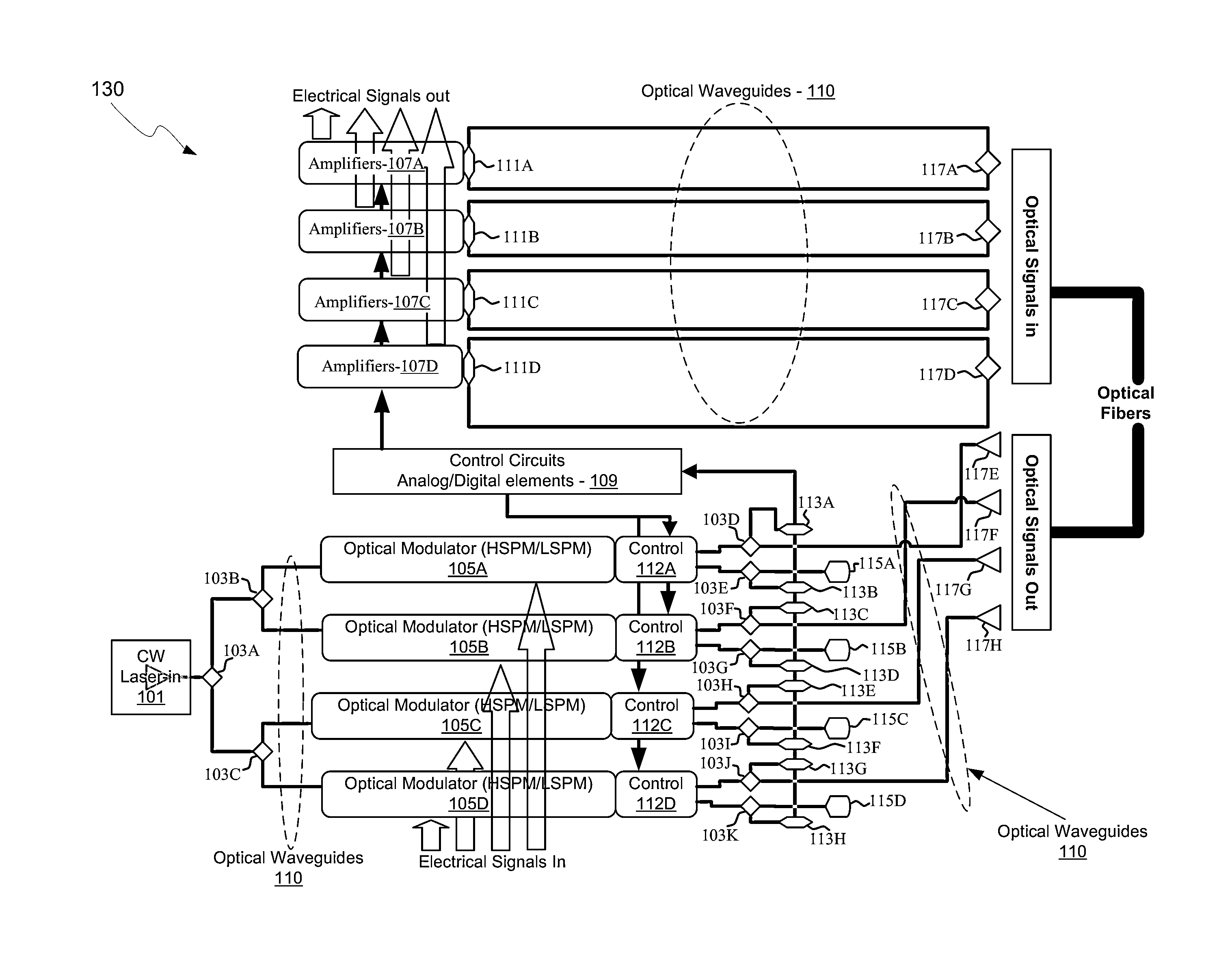
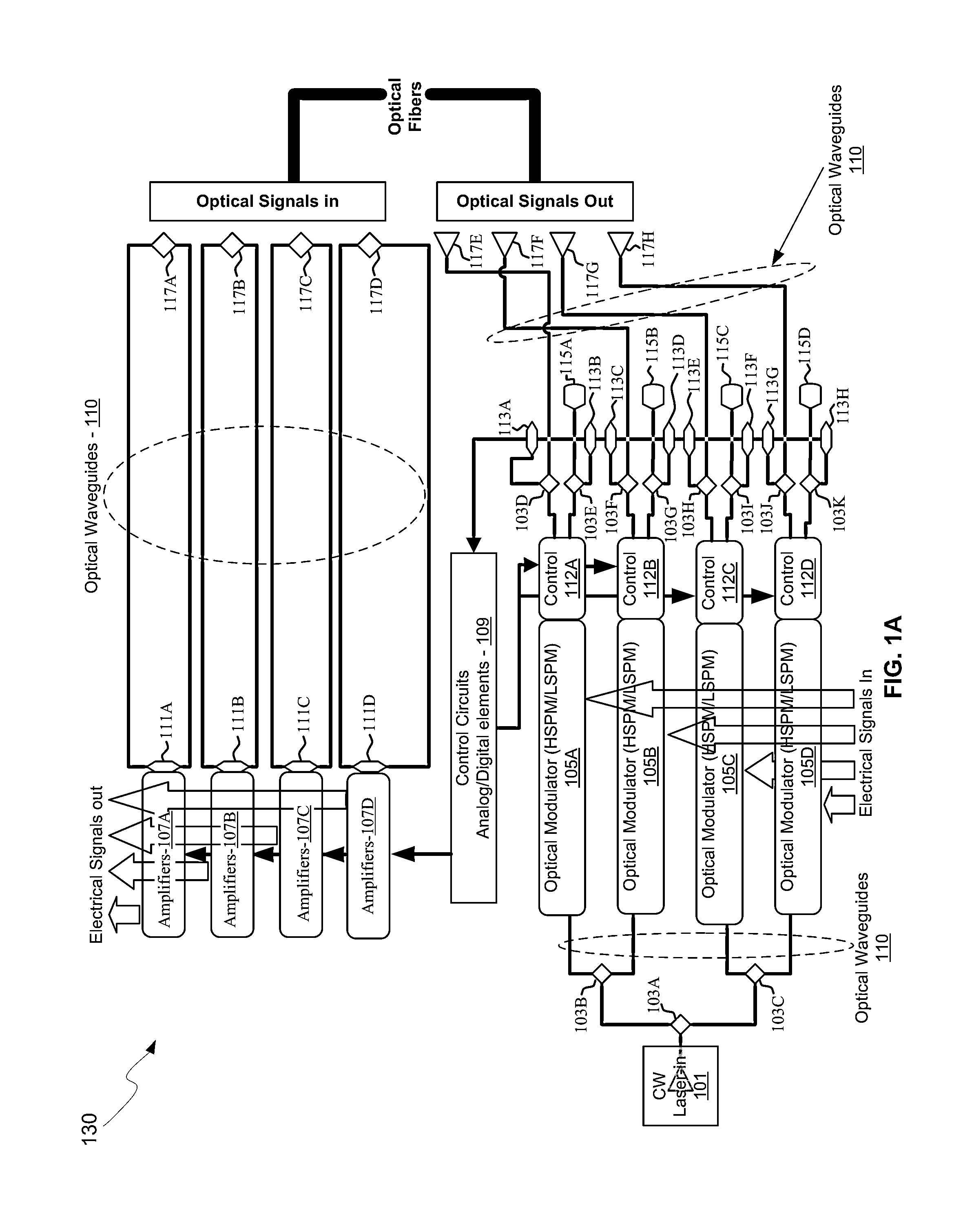
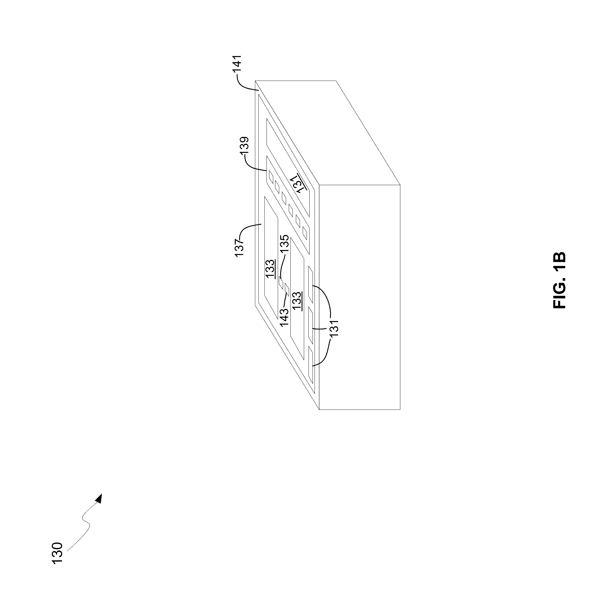
[0015]Certain aspects of the disclosure may be found in a method and system for a low-loss optical Y-Junction power splitter. Exemplary aspects of the disclosure may comprise in a semiconductor die with an optical Y-junction, where the optical Y-junction comprises an input waveguide, two or more output waveguides, a taper region and a step feature. The input waveguide and the taper region may include a smooth transition between them, and the step feature may be between the taper region and the two or more output waveguides. The semiconductor die may receive an optical signal in the input waveguide, and communicate substantially equal power optical signals to each of the two or more output waveguides. The semiconductor die may comprise a photonically-enabled integrated circuit. The semiconductor die may comprise silicon. An optical signal may be received in each of the two or more output waveguides and a summed output signal may be communicated to the input waveguide. The semiconduct...


PUM


Abstract

Methods and systems for a low-loss optical Y-Junction power splitter are disclosed and may include a semiconductor die having an optical Y-junction. The optical Y-junction may comprise an input waveguide, two or more output waveguides, a taper region and a step feature. The input waveguide and the taper region may include a smooth transition between the input waveguide and the taper region, and the step feature may be between the taper region and the output waveguides. The semiconductor die may receive an optical signal in the input waveguide, and communicate substantially equal power optical signals to the output waveguides. The semiconductor die may comprise a photonically-enabled silicon CMOS integrated circuit. An optical signal may be received in each of the output waveguides and a summed output signal may be communicated to the input waveguide. The step feature may extend in a direction perpendicular to an axis of the output waveguides. Widths of the output waveguides may be different and define a splitting ratio of the Y-junction.

Description

CROSS-REFERENCE TO RELATED APPLICATIONS / INCORPORATION BY REFERENCE[0001]This application claims priority to and the benefit of U.S. Provisional Application 61 / 995,302 filed on Apr. 7, 2014, which is hereby incorporated herein by reference in its entirety.FIELD[0002]Certain embodiments of the disclosure relate to semiconductor photonics. More specifically, certain embodiments of the disclosure relate to a method and system for a low-loss optical Y-Junction power splitter.BACKGROUND[0003]As data networks scale to meet ever-increasing bandwidth requirements, the shortcomings of copper data channels are becoming apparent. Signal attenuation and crosstalk due to radiated electromagnetic energy are the main impediments encountered by designers of such systems. They can be mitigated to some extent with equalization, coding, and shielding, but these techniques require considerable power, complexity, and cable bulk penalties while offering only modest improvements in reach and very limited s...

Claims


Application Information

Patent Timeline
Patent Type & Authority Applications(United States)
IPC IPC(8): G02B6/28
CPCG02B6/2804G02B6/2808
Inventor MEKIS, ATTILAVERSLEGERS, LIEVEN
Owner CISCO TECH INC
Why Eureka
Try Eureka