Spacer formation

a technology of spacers and forming methods, applied in the direction of basic electric elements, semiconductor/solid-state device manufacturing, electric devices, etc., can solve the problem that the photolithographic technique may not be reliably formed

Active Publication Date: 2015-10-08
APPLIED MATERIALS INC
View PDF2 Cites 290 Cited by
  • Summary
  • Abstract
  • Description
  • Claims
  • Application Information

AI Technical Summary

Benefits of technology

[0004]Embodiments of the present invention pertain to methods of forming more symmetric spacers which may be used for self-aligned multi-patterning processes. A conformal spacer layer of spacer material is formed over mandrels patterned near the optical resolution of a photolithography system using a high-resolution photomask. A carbon-cont...

Problems solved by technology

Due to factors such as optics and light or radiation wavelength, however, photolithography technique...

Method used


Image

  • Spacer formation
  • Spacer formation
  • Spacer formation

Examples


Embodiment Construction

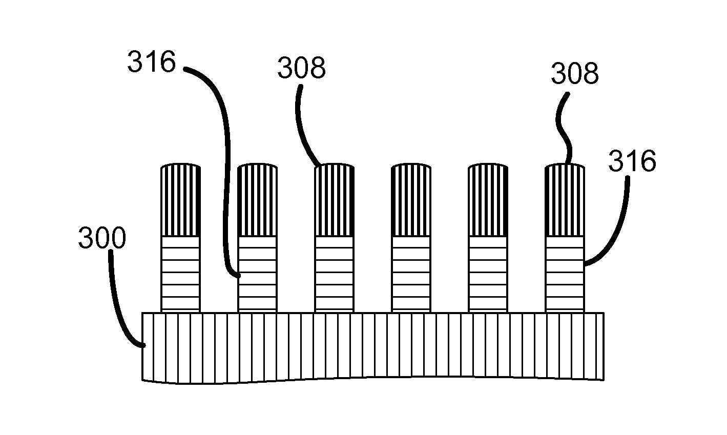
[0014]Embodiments of the present invention pertain to methods of forming more symmetric spacers which may be used for self-aligned multi-patterning processes. A conformal spacer layer of spacer material is formed over mandrels patterned near the optical resolution of a photolithography system using a high-resolution photomask. A carbon-containing layer is further formed over the conformal spacer layer. The carbon-containing layer is anisotropically etched to expose the high points of the conformal spacer layer while retaining carbon side panels. The conformal spacer layer may then be etched to form spacers without the traditional skewing of the profile towards one side or the other.

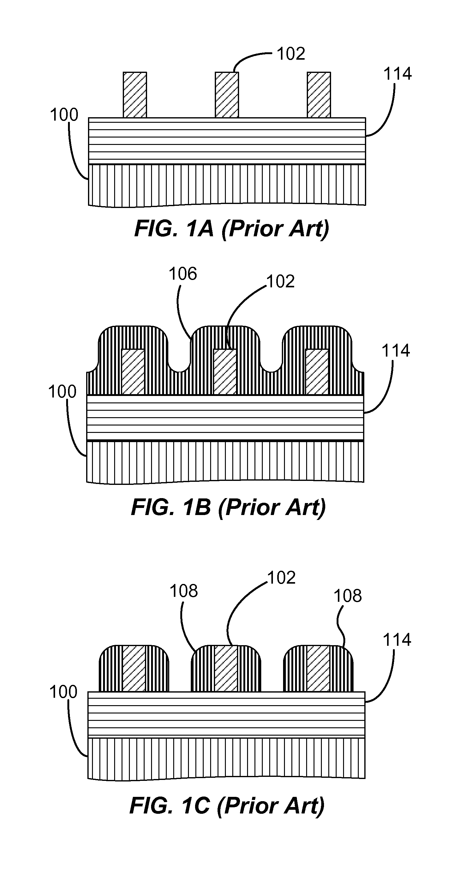
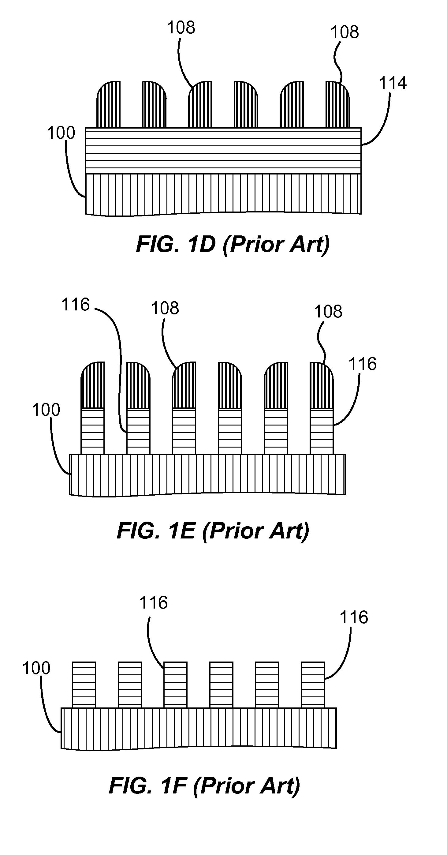
[0015]Using the prior art discussed previously with reference to FIGS. 1A-1F has been found to produce alternating shapes of spacers 108, while one slopes down to the left, an adjacent spacer slopes down to the right. The alternating slopes of spacers 108 have been linked with undesirable alternating vari...


PUM


Abstract

Embodiments of the present invention pertain to methods of forming more symmetric spacers which may be used for self-aligned multi-patterning processes. A conformal spacer layer of spacer material is formed over mandrels patterned near the optical resolution of a photolithography system using a high-resolution photomask. A carbon-containing layer is further formed over the conformal spacer layer. The carbon-containing layer is anisotropically etched to expose the high points of the conformal spacer layer while retaining carbon side panels. The conformal spacer layer may then be etched to form spacers without the traditional skewing of the profile towards one side or the other.

Description

FIELD[0001]Embodiments of the present invention relate to methods of forming spacers.BACKGROUND OF THE INVENTION[0002]Shrinking integrated circuits (ICs) result in improved performance, increased capacity and / or reduced cost per transistor. Each device shrink requires more sophisticated techniques to form the features. Photolithography is commonly used to pattern features on a substrate. An exemplary feature is a line of a material which may be a metal, semiconductor or insulator. Linewidth is the width of the line and the spacing is the distance between adjacent lines. Pitch is defined as the distance between a same point on two neighboring lines. The pitch is equal to the sum of the linewidth and the spacing. Due to factors such as optics and light or radiation wavelength, however, photolithography techniques have a minimum pitch below which a particular photolithographic technique may not reliably form features. Thus, the minimum pitch of a photolithographic technique can limit f...

Claims


Application Information

Patent Timeline
IPC IPC(8): H01L21/311
CPCH01L21/0274H01L21/31138H01L21/31144H01L21/3086H01L21/0337H01L21/31116H01L21/31122H01L21/32139
Inventor LUERE, OLIVIERKANG, SEAN S.NEMANI, SRINIVAS D.
Owner APPLIED MATERIALS INC
Why Eureka
Try Eureka