Semiconductor device

Inactive Publication Date: 2015-10-15
TOYOTA JIDOSHA KK
View PDF4 Cites 3 Cited by
  • Summary
  • Abstract
  • Description
  • Claims
  • Application Information

AI Technical Summary

Benefits of technology

[0003]However, when the fuse portion has blown out to break off the conduction path, the conventional technology cannot sense the break-off of the conduction path. For this reason, for example, if the conventional technology is applied to a semicondu

Problems solved by technology

However, in such semiconductor devices, a capacitor failure caused by short-circuit

Method used


Image

  • Semiconductor device
  • Semiconductor device
  • Semiconductor device

Examples


Example

Embodiment 1

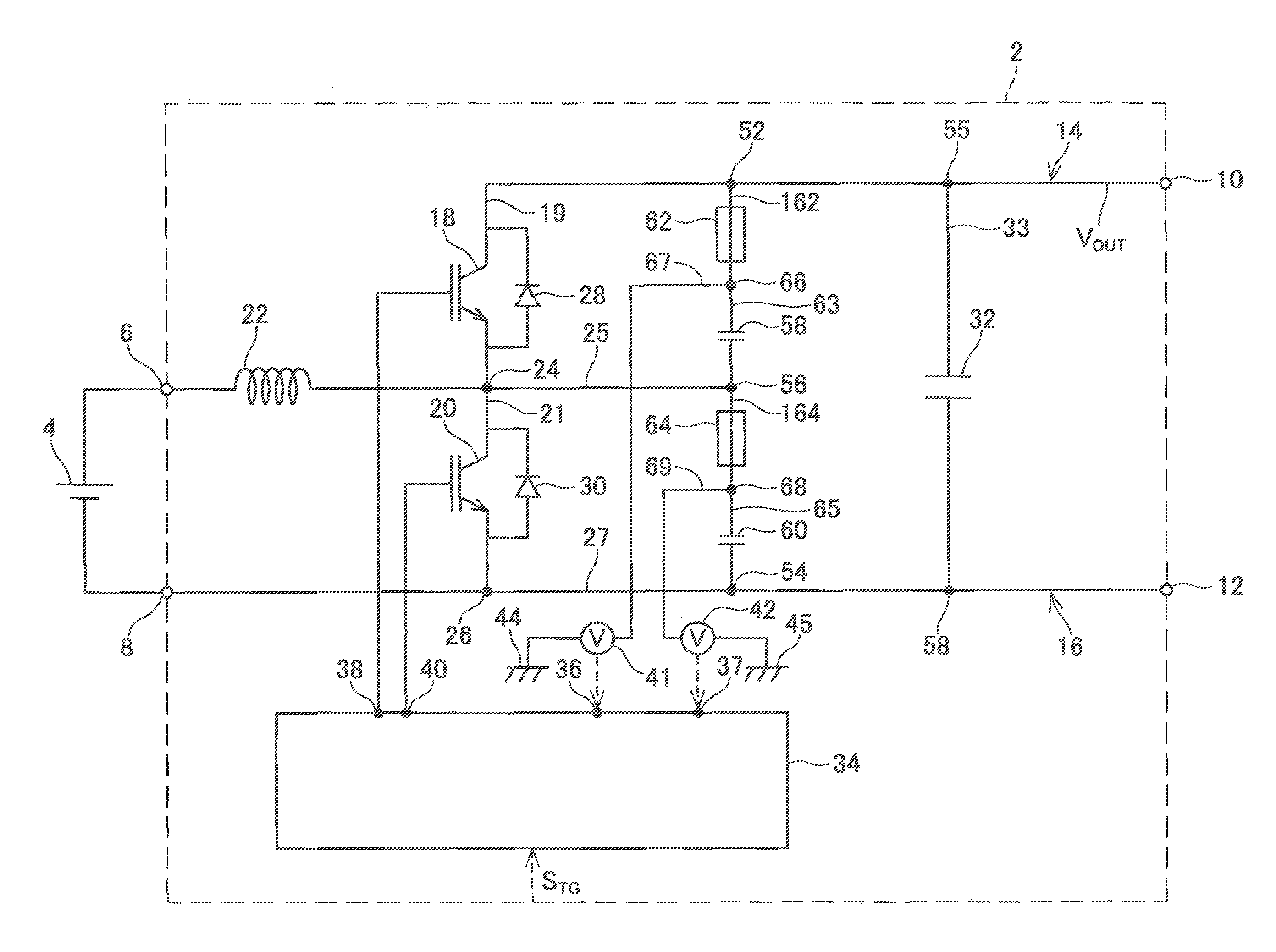
[0025]A DC-DC converter 2 raises an input voltage inputted from a battery 4. As shown in FIG. 1, the DC-DC converter 2 outputs an output voltage to a load (not illustrated). The load is for example an inverter (not illustrated) or the like.

[0026]A configuration of the DC-DC converter 2 of the present embodiment is described below. The DC-DC converter 2 includes an input terminal 6 and an input-side reference terminal 8. The input terminal 6 is connected to a positive electrode of the battery 4. The input-side reference terminal 8 is connected to a negative electrode of the battery 4. That is, an input voltage is inputted between the input terminal 6 and the input-side reference terminal 8. Further, the input-side reference terminal 8 is connected to the ground. The DC-DC converter 2 includes an output terminal 10 and an output-side reference terminal 12. The output terminal 10 is connected, for example, to an input terminal (not illustrated) on a positive electrode side ...

Example

Embodiment 2

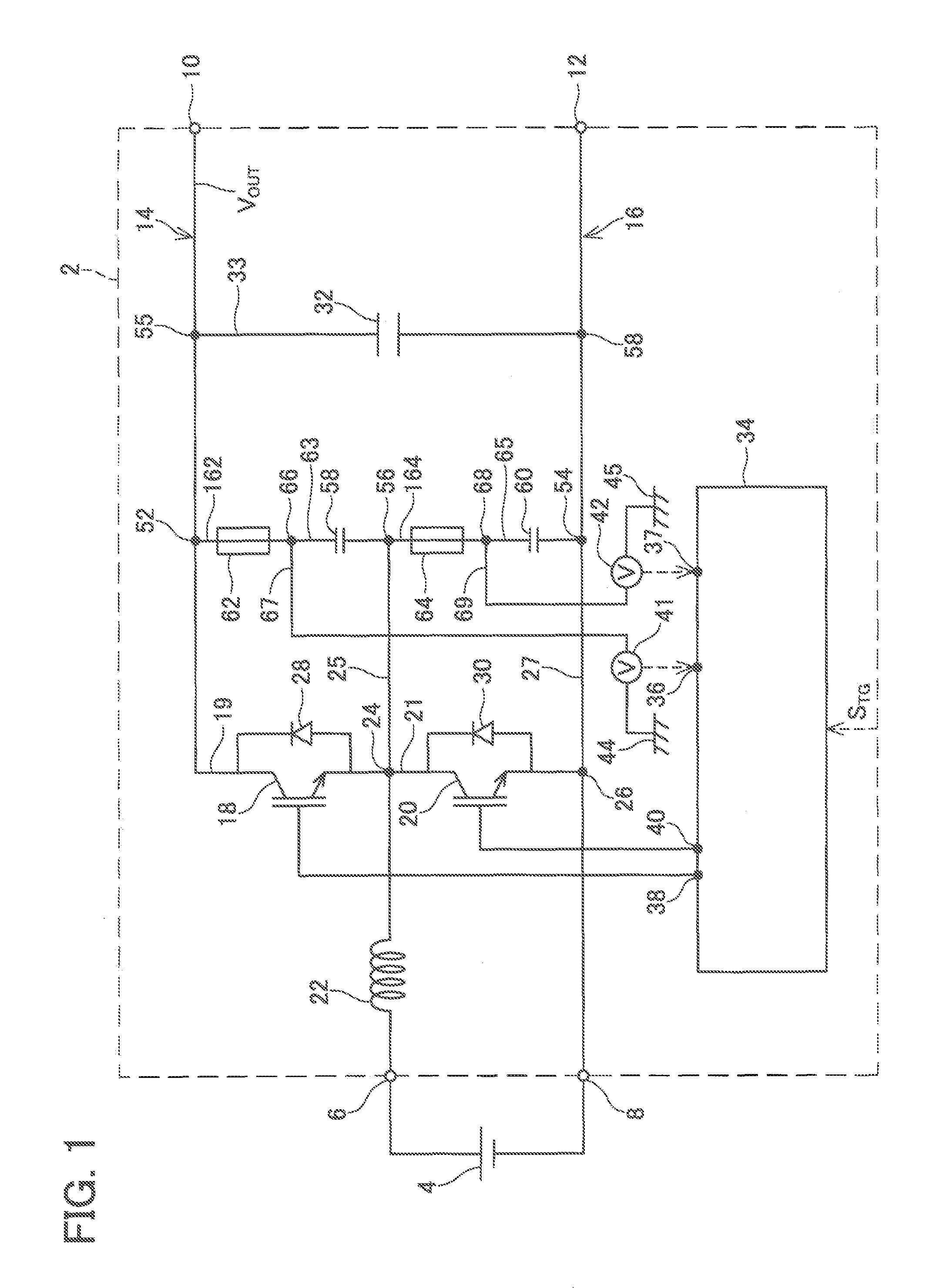
[0055]In a DC-DC converter 202 of Embodiment 2, a connection point 86 is provided on the input / output line 14. The connection point 86 is positioned on an output terminal 10 side of the first switching element 18. Further, the connection point 86 is positioned between the first switching element 18 and the connection point 55. A connection point 88 is provided on the reference potential line 16. The connection point 88 is positioned on an output reference terminal 12 side of the connection point 26. The connection point 88 is positioned between the connection point 26 and the connection point 58. A wiring 83 connects the connection point 86 and the connection 88. That is, the wiring 83 is set in parallel to the first switching element 18 and the second switching element 20. A capacitor 80 is set on the wiring 83. In other words, the capacitor 80 is set in parallel to the first switching element 18 and the second switching element 20.

[0056]A fuse portion 82 is provided on...


PUM


Abstract

A semiconductor device presented herein includes a first wiring including a first end and a second end configured to receive a voltage lower than a voltage of the first end. The semiconductor device includes a second wiring including a third end connected to the first end, and a fourth end connected to the second end. The semiconductor device includes a switching element set on the first wiring, a capacitor set on the second wiring, and a fuse portion set on the second wiring and positioned on a third end side of the capacitor. The semiconductor device includes a potential sensing portion connected to the second wiring between the fuse portion and the capacitor and configured to sense a potential of a connection point thereof.

Description

TECHNICAL FIELD[0001]A technology disclosed herein relates o semiconductor devices.BACKGROUND ART[0002]In a semiconductor device including a semiconductor element such as a switching element or a diode, a capacitor may be provided in parallel to the semiconductor element. The capacitor for example achieves a reduction in a surge voltage that is applied to the semiconductor element. However, in such semiconductor devices, a capacitor failure caused by short-circuiting may cause an overcurrent to flow through a wiring on which the capacitor is set. Japanese Patent Application Publication No. H1-103163 A discloses a semiconductor device in which a capacitor is provided in parallel to a diode. In this semiconductor device, a fuse portion (blowout pattern) is provided as a part of a junction electrode pattern of the capacitor. When the capacitor fails by short-circuiting, the fuse portion blows out to break off a conduction path. This makes it possible to reduce the risk of the overcurre...

Claims


Application Information

Patent Timeline
IPC IPC(8): H02M1/32H02M3/337H01L23/528H01L27/06H01L23/525
CPCH02M1/32H01L27/0629H02M2001/325H01L23/528H02M3/337H01L23/5256H02M3/155H02M3/158H02M1/325
Inventor IMAI, MAKOTO
Owner TOYOTA JIDOSHA KK
Why Eureka
Try Eureka