Semiconductor memory device

Inactive Publication Date: 2015-10-22
SK HYNIX INC
View PDF5 Cites 0 Cited by
  • Summary
  • Abstract
  • Description
  • Claims
  • Application Information

AI Technical Summary

Benefits of technology

The present invention provides a semiconductor memory device that can store data in multiple ways for stable readout. The device includes three memory regions, each containing multiple memory cells that can be selected simultaneously by a single address. The first region stores a single datum, the second region stores two single data, and the third region stores three single data. This design allows for efficient data storage and retrieval.

Problems solved by technology

Since the charge capacity of the capacitor C and the voltage sweeping range of the bit line BL become smaller, the data may not be stably readout.

Method used


Image

  • Semiconductor memory device
  • Semiconductor memory device
  • Semiconductor memory device

Examples


Embodiment Construction

[0025]Exemplary embodiments of the present invention are described below in more detail with reference to the accompanying drawings. These embodiments are provided so that this disclosure is thorough and complete and fully conveys the scope of the present invention to those skilled in the art.

[0026]The accompanying drawings and the related description only show part of circuits as an example for clear description of the present invention, and therefore the scope of the present invention will not be limited by the examples of the description and the accompanying drawings but by the claims.

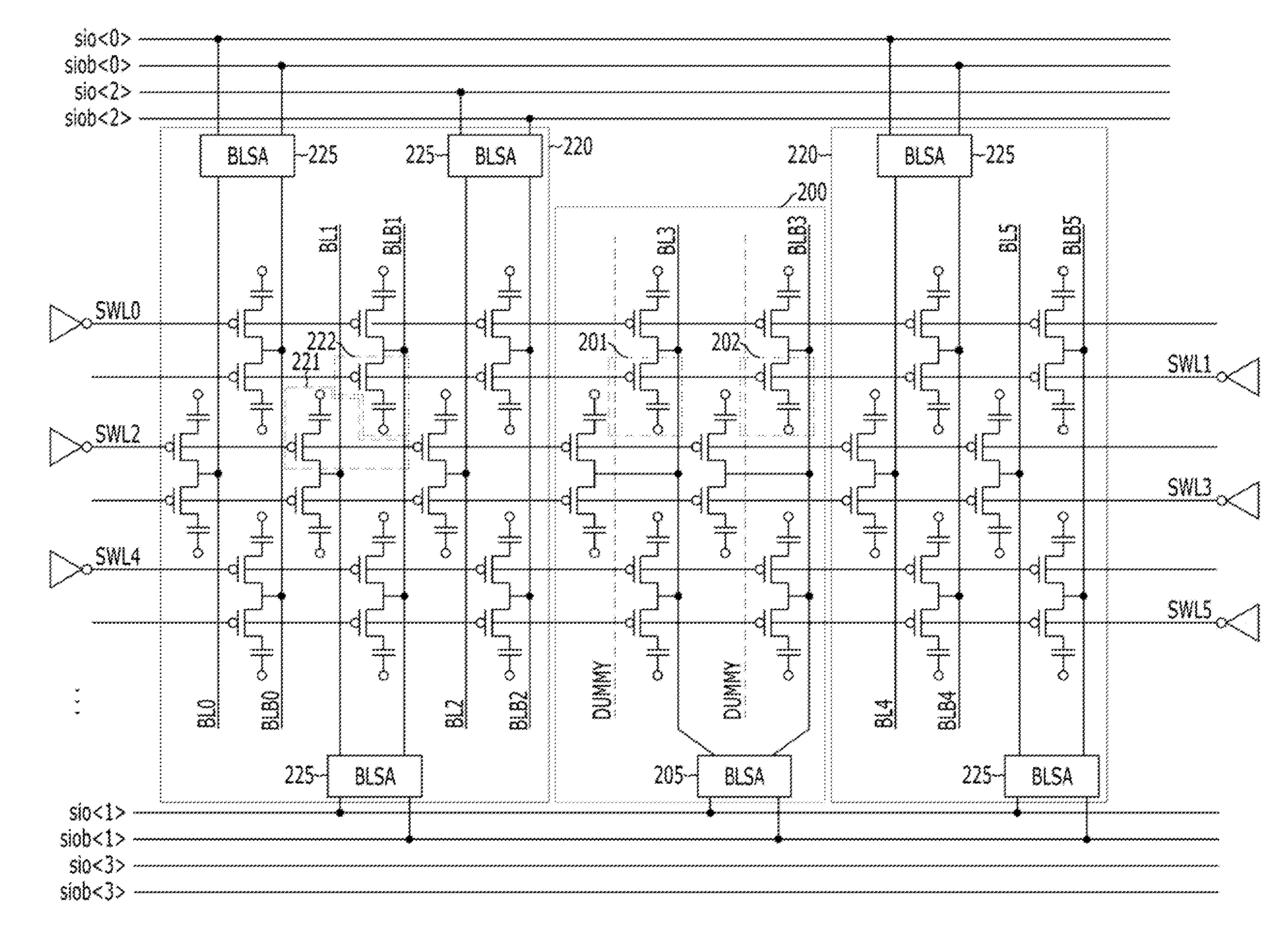
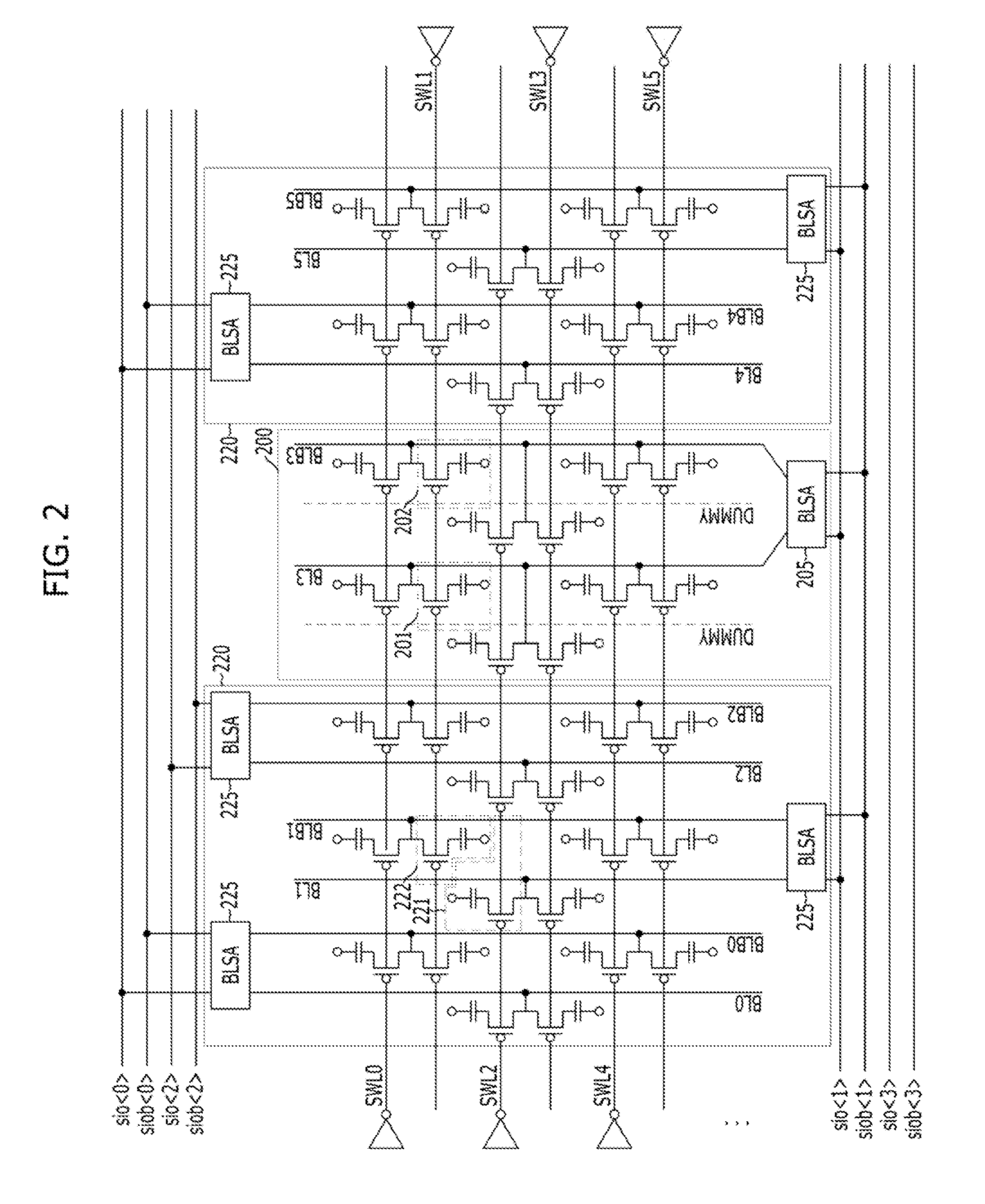
[0027]FIG. 2 a circuit diagram illustrating a memory cell array of a semiconductor memory device in accordance with an exemplary embodiment of the present invention.

[0028]Referring to FIG. 2, the memory cell array of the semiconductor memory device may include first and second memory regions 200 and 220. For example, the first memory region 200 may include a weighted sense amplifier 205, first and s...


PUM


Abstract

A semiconductor memory device includes: a first memory region including a plurality of first memory cells, two or more of which are simultaneously selected by a single address, and stores a first single datum; and a second memory region including a plurality of second memory cells, each of which is selected by the single address, and stores a second single datum.

Description

CROSS-REFERENCE TO RELATED APPLICATIONS[0001]The present application claims priority of Korean Patent Application No. 10-2014-0047838, filed on Apr. 22, 2014, which is incorporated herein by reference in its entirety.BACKGROUND[0002]1. Field[0003]Various exemplary embodiments of the present invention relate to a semiconductor design technology, and more particularly, to a semiconductor memory device capable of selectively securing stable data readout.[0004]2. Description of the Related Art[0005]In general, a semiconductor memory device includes a plurality of memory cells, each of which stores data representing ‘0’ or ‘1’.[0006]FIG. 1 is a schematic diagram illustrating a memory cell of a typical semiconductor memory device.[0007]FIG. 1 shows a memory cell of a general Dynamic Random Access Memory (DRAM) of 1-transistor-1-capacitor (1T1C) structure.[0008]The transistor TR of the memory cell turns on / off coupling between a bit line BL and the capacitor C in response to a signal on a ...

Claims


Application Information

Patent Timeline
IPC IPC(8): G11C5/02G11C7/06G11C5/06
CPCG11C5/025G11C7/06G11C5/063G11C11/408G11C11/4091G11C11/4097G11C2211/4013
Inventor KIM, KWAN-WEON
Owner SK HYNIX INC
Why Eureka
Try Eureka