Supercharge Your Innovation With Domain-Expert AI Agents!

Image sensor with floating diffusion interconnect capacitor

Active Publication Date: 2015-11-05
SONY CORP +1
View PDF13 Cites 14 Cited by
  • Summary
  • Abstract
  • Description
  • Claims
  • Application Information

AI Technical Summary

Benefits of technology

The present invention relates to a new pixel layout for an image sensor. The technical effects of the invention are related to the layout of the local interconnect which connects a charge storage node to a readout node. The invention provides a layout that optimizes the connection between the various pixel elements, resulting in improved image quality and reduced noise. The layout includes various elements such as the gate electrodes, transfer gate lines, readout select lines, and power supply lines, among others. The layout also includes different layers in which the various wiring lines are located. Overall, the invention provides a more efficient and effective image sensor for capturing high-quality images.

Problems solved by technology

In global shutter mode, however, this time can be easily several milliseconds.
This dark signal increases FPN and temporal noise.

Method used


Image

  • Image sensor with floating diffusion interconnect capacitor
  • Image sensor with floating diffusion interconnect capacitor
  • Image sensor with floating diffusion interconnect capacitor

Examples


Embodiment Construction

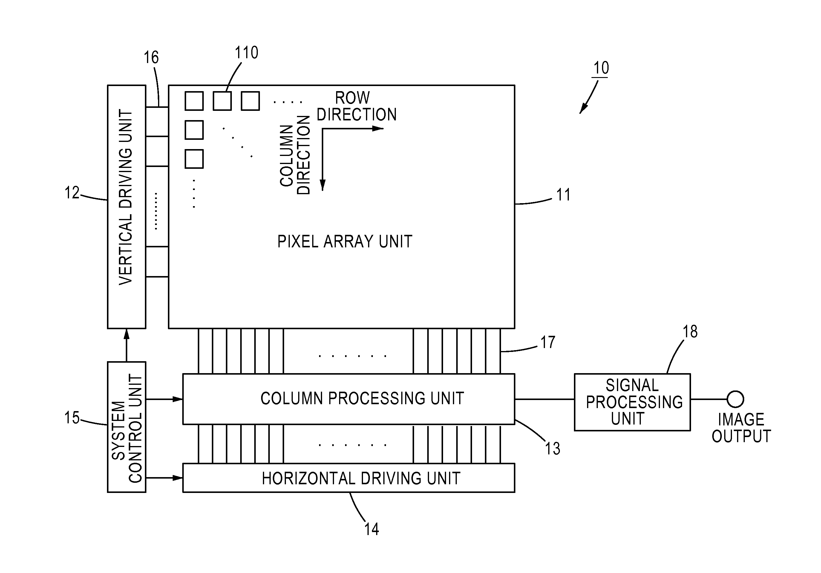
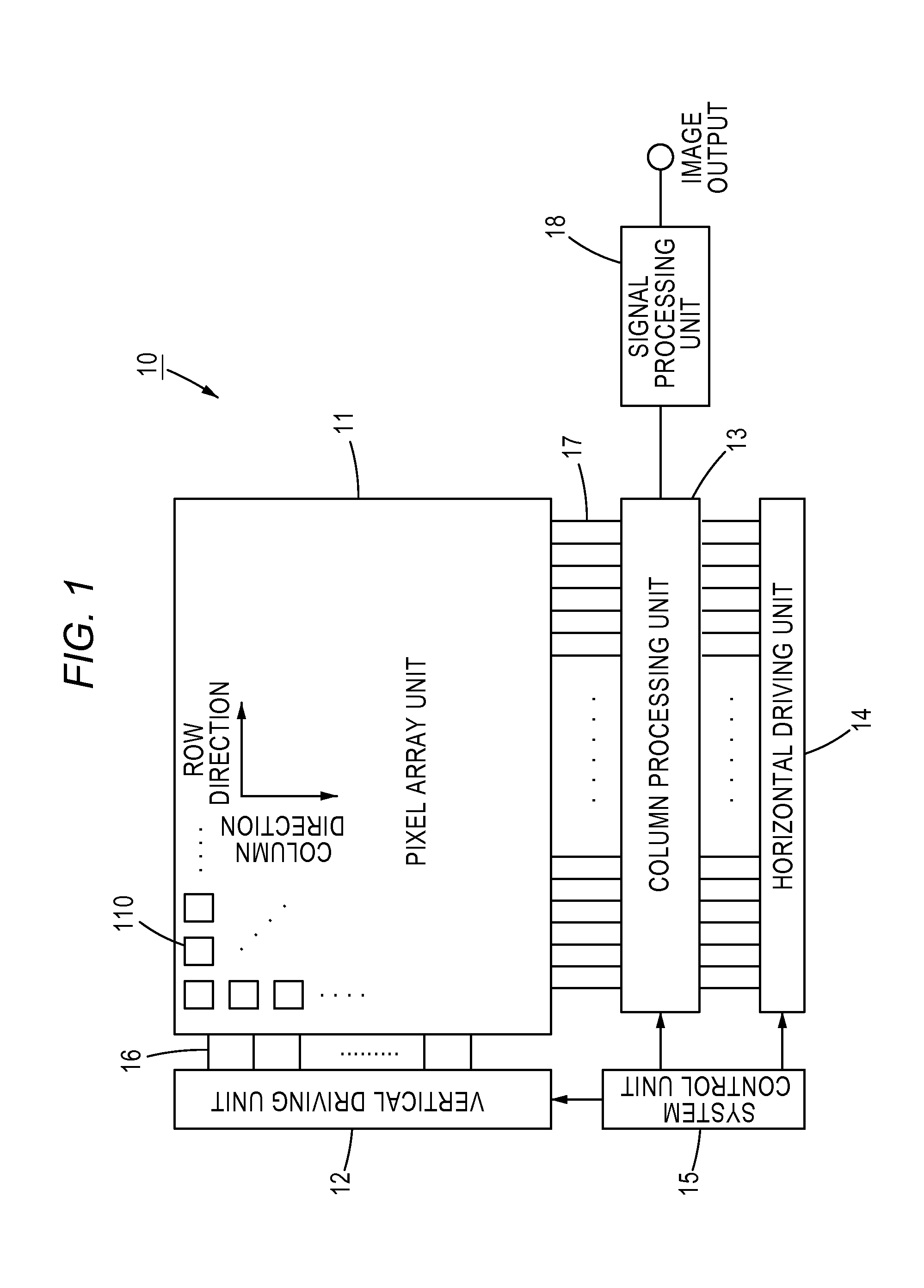
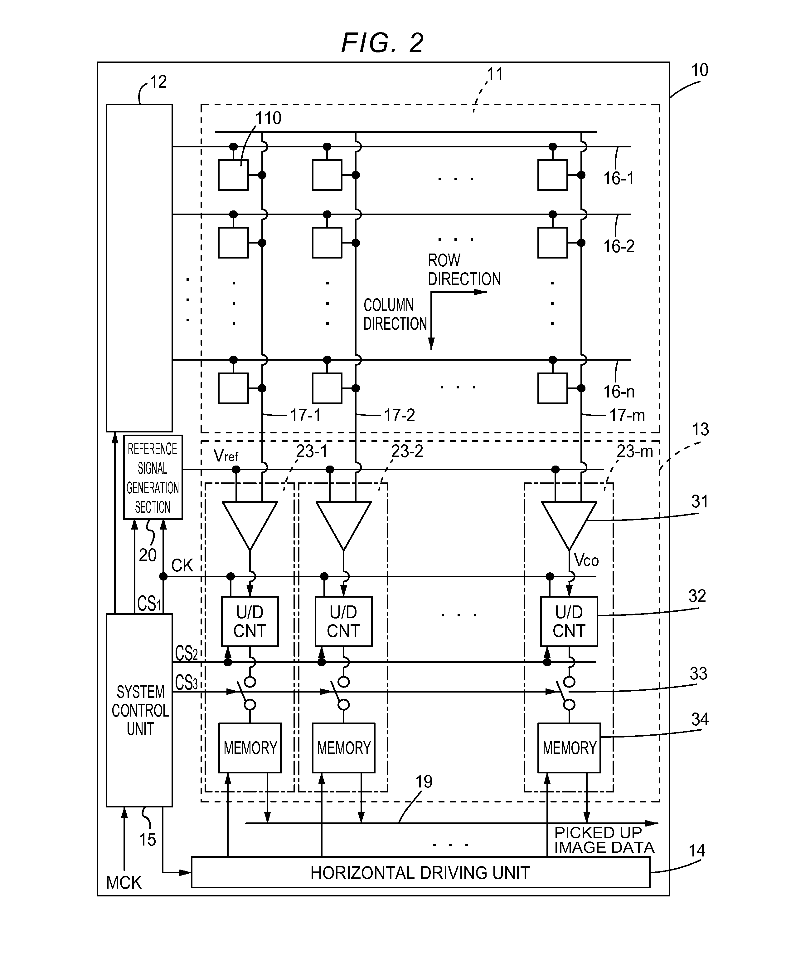
[0024][Image Sensor—General Configuration]

[0025]FIGS. 1 and 2 illustrates an exemplary CMOS image sensor 10. The image sensor 10 is formed on a semiconductor substrate 700 (for example, silicon substrate 700 as shown in FIGS. 7A and 7B). The image sensor 10 includes a pixel region 11 in which pixels 110 are arranged, for example, in an x m matrix shape having n rows and m columns. The pixel region 11 may include an effective pixel region (not illustrated) and an optical black pixel region (not illustrated). Pixels 110 in the effective pixel region are for outputting pixel signals which correspond to the bits (also called dots or pixels) of an image created by the image sensor. Pixels in the optical black region, on the other hand, are for outputting black level signals used as a reference for various noise cancellation techniques. Pixels in the optical black region are generally identical to the pixels 110 in the effective pixel region except that they are shielded from incident lig...


PUM


Abstract

An image sensor includes a pixel circuit that includes a light sensing element and a charge storage node formed in a substrate, an output element having a control electrode formed in an electrode layer above the substrate, the output element generating an output signal corresponding to charge generated by the light sensing element and held by the charge storage node, and a local metal interconnect that electrically connects the charge storage node to the control electrode. Control wirings that control operations of the pixel circuit are formed in wiring layers that are located above the electrode layer. The metal interconnect is formed in a layer that is located above the electrode layer and below a lowest one of the wiring layers such that a given one of the control wirings overlaps the metal interconnect so as to form a parallel plate capacitor in a region of overlap.

Description

BACKGROUND[0001]1. Technical Field[0002]The invention relates to image sensor systems and, in particular although not exclusively, to active pixel CMOS image sensors implementing an electronic global shutter.[0003]2. Background Art[0004]Digital image capturing devices use image sensors to convert incident light energy into electrical signals. An image sensor includes a two-dimensional array of light sensing elements called pixels. For example, a CMOS image sensor includes an n x m array of photosensitive structures (for example, photodiodes) as well as circuit elements for readout and control (a photodiode plus its immediate readout and control transistors are typically called a “pixel”). Each pixel in the array produces an electrical signal corresponding to an amount of light incident upon the pixel during an integration period. Outputs from the light sensing elements are converted to digital form and stored digitally to form raw data representing a scene. The raw data can be proce...

Claims


Application Information

Patent Timeline
IPC IPC(8): H04N5/369
CPCH04N5/369H01L27/14603H01L27/14612H01L27/14621H01L27/14627H01L27/14636H01L27/14638H04N25/77
Inventor BRADY, FREDERICKHWANG, SUNGINAYERS, THOMAS R.
Owner SONY CORP
Features
  • R&D
  • Intellectual Property
  • Life Sciences
  • Materials
  • Tech Scout
  • Unparalleled Data Quality
  • Higher Quality Content
  • 60% Fewer Hallucinations
Learn More