3D stacked IC device with stepped substack interlayer connectors

a technology of interlayer connectors and ic devices, which is applied in the direction of semiconductor devices, semiconductor/solid-state device details, electrical apparatus, etc., can solve the problems of increasing the number of lithographic steps, increasing the cost of interconnection implementation, and increasing the number of layers

Active Publication Date: 2015-11-12
MACRONIX INT CO LTD
View PDF2 Cites 41 Cited by
  • Summary
  • Abstract
  • Description
  • Claims
  • Application Information

AI Technical Summary

Problems solved by technology

The cost to implement the interconnections increases with the number of lithographic steps needed.
However, limitations can arise as the number of layers increases, because not only does the number of etch steps increase even using binary system etch approaches, but also the depths of the required vias increase.
With greater depths, the layout area for each interlayer connector can increase and process control issues arise.

Method used


Image

  • 3D stacked IC device with stepped substack interlayer connectors
  • 3D stacked IC device with stepped substack interlayer connectors
  • 3D stacked IC device with stepped substack interlayer connectors

Examples


Embodiment Construction

[0020]A detailed description of embodiments of the present invention is provided with reference to the FIGS. 1-31.

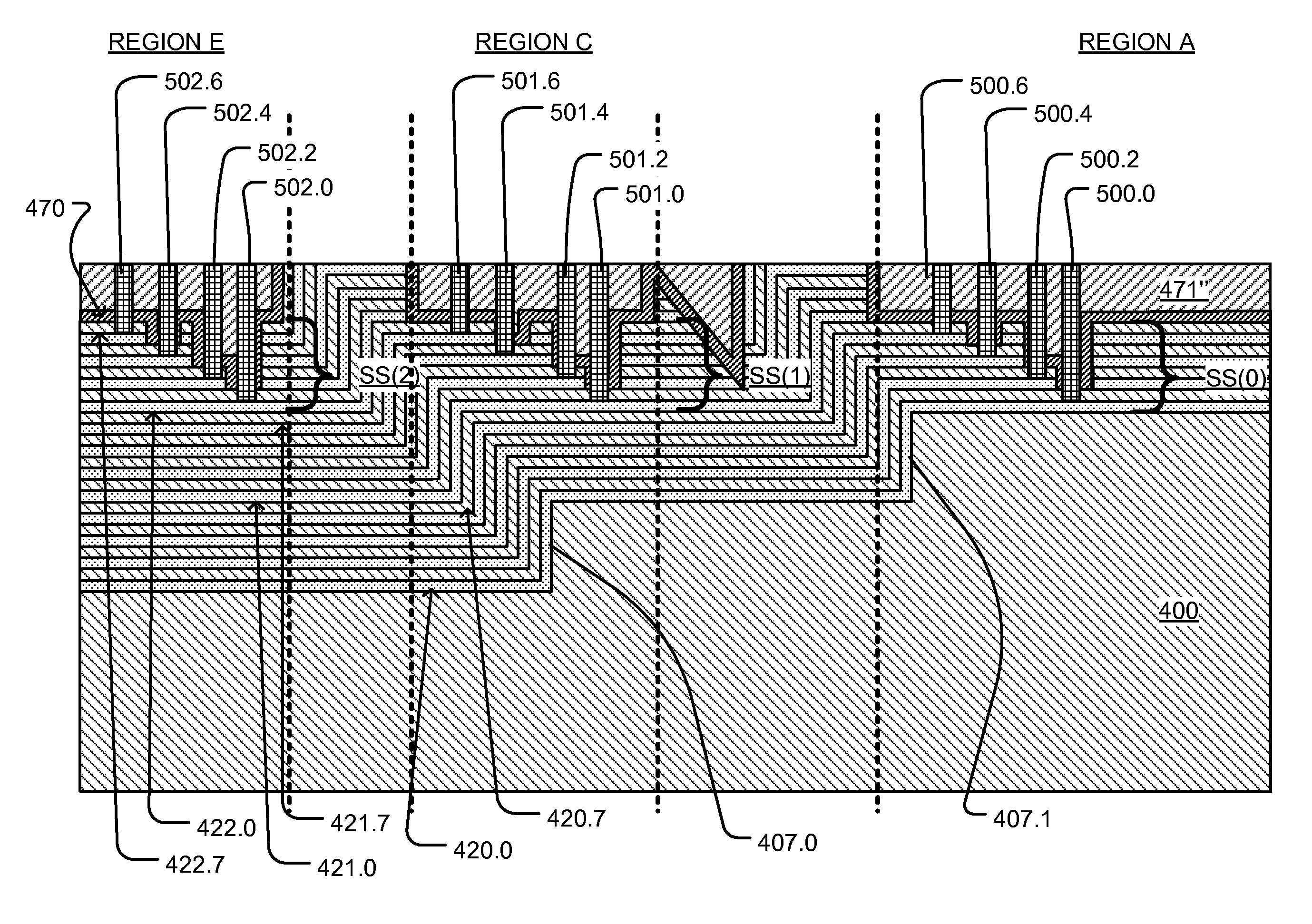
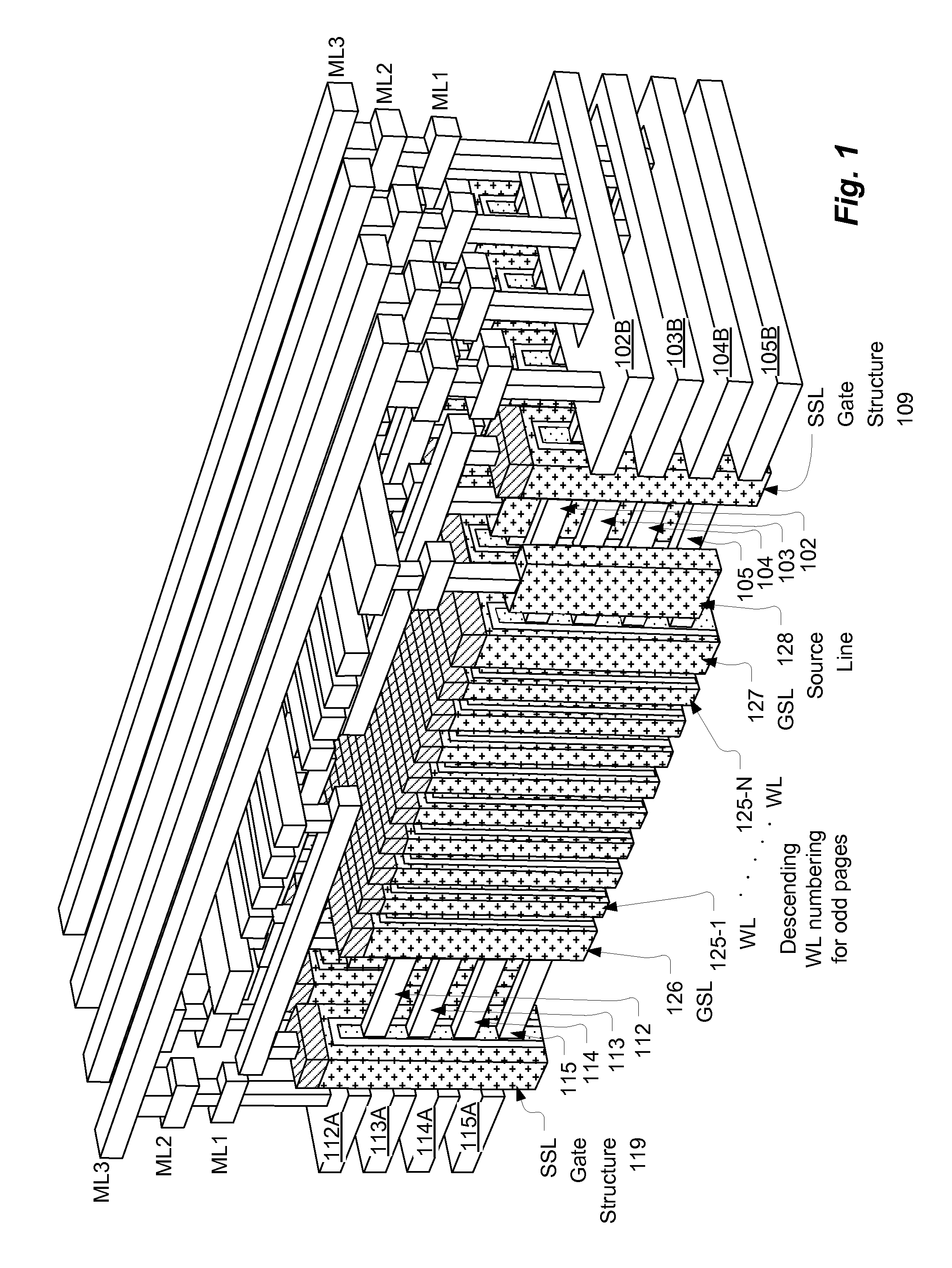
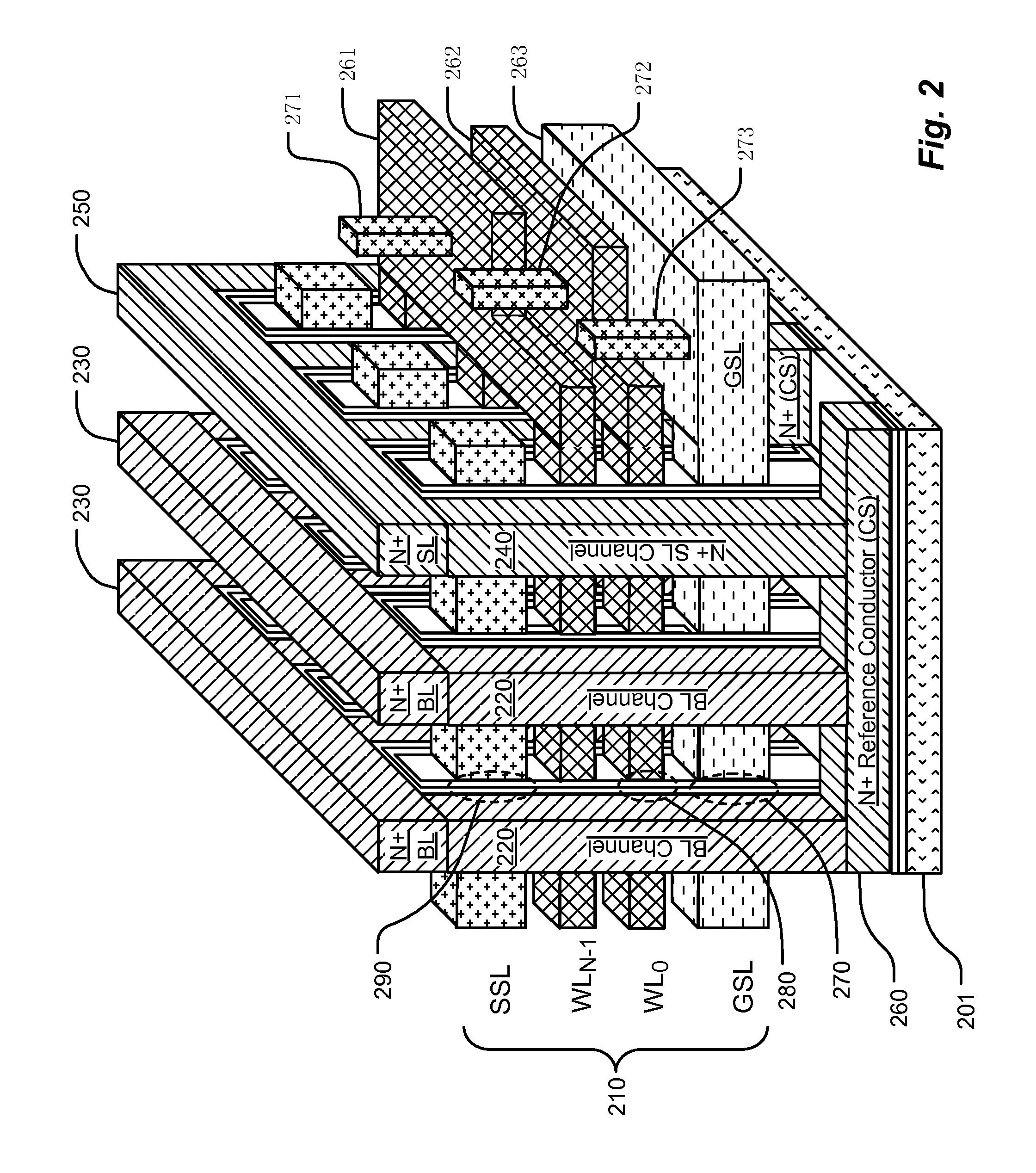
[0021]FIG. 1 is a perspective illustration of a three-dimensional (3D) NAND-flash memory device which includes contact pads at which interlayer connectors contact the corresponding active layers. The device illustrated in FIG. 1 includes stacks of active lines in active layers of the array, alternating with insulating lines. Insulating material is removed from the drawing to expose additional structure. For example, insulating lines are removed between the semiconductor lines in the stacks, and between the stacks of semiconductor lines. This structure is described herein in some detail, as an example of a three-dimensional (3D) memory array which can be manufactured in a recessed area, or pit, on a semiconductor substrate, in combination with peripheral circuits on the substrate outside of the pit. In some embodiments, the structure shown in FIG. 1 is not manufactured in...


PUM


Abstract

A stepped substack interlayer connector structure on a multilayer integrated circuit includes N steps on the substrate from a surface of the substrate at a first level to a surface of the substrate at a second level. A stack of active layers alternating with insulating layers on the substrate, including a plurality of substacks disposed in relation to the N step(s) to form respective contact regions in which the substacks are disposed at a common level. Interlayer connectors are formed by conductors in the respective regions connected to landing areas on active layers in each of the plurality of substacks. The maximum depth of the interlayer connectors is equal to, or less than, the thickness of one of the substacks.

Description

BACKGROUND OF THE INVENTION[0001]1. Field of the Invention[0002]The present invention relates to interlayer connectors for multi-layer integrated circuits and the like, including high density three-dimensional (3D) memory devices.[0003]2. Description of Related Art[0004]In the manufacturing of high density memory devices, the amount of data per unit area on an integrated circuit can be a critical factor. Thus, as the critical dimensions of the memory devices approach lithographic technology limits, techniques for stacking multiple levels or layers of memory cells have been proposed in order to achieve greater storage density and lower costs per bit.[0005]For example, thin film transistor techniques are applied to charge trapping memory in Lai, et al., “A Multi-Layer Stackable Thin-Film Transistor (TFT) NAND-Type Flash Memory,” IEEE Int'l Electron Devices Meeting, 11-13 Dec. 2006; and in Jung et al., “Three Dimensionally Stacked NAND Flash Memory Technology Using Stacking Single Crys...

Claims


Application Information

Patent Timeline
Patent Type & Authority Applications(United States)
IPC IPC(8): H01L27/115H01L23/522H01L21/768H01L23/528
CPCH01L27/11578H01L21/76877H01L23/5226H01L23/528H01L2924/0002H10B43/50H10B43/27H01L2924/00H10B43/20
Inventor CHEN, SHIH-HUNG
Owner MACRONIX INT CO LTD
Why Eureka
Try Eureka