
Light emitting device

Inactive Publication Date: 2015-11-12
GENESIS PHOTONICS
View PDF6 Cites 19 Cited by
  • Summary
  • Abstract
  • Description
  • Claims
  • Application Information

AI Technical Summary

Benefits of technology

The invention is a light emitting device with larger electrode area, which improves the accuracy of assembly alignment when attaching to an external circuit. The device has electrodes that extend out from the epitaxial structure layer and may cover at least a portion of the encapsulant, making it easier to align and bond with the external circuit. This design also allows for improved alignment accuracy in the chip bonding process.

Problems solved by technology

In case of such configuration, when the flip-chip LED package is to be assembled to an external circuit, since an electrode area of the N electrode and the P electrode is relative small, the LED package may have problems of inaccurate alignment and poor electrode contact in assembling.

Method used


Image

  • Light emitting device
  • Light emitting device
  • Light emitting device

Examples


Embodiment Construction

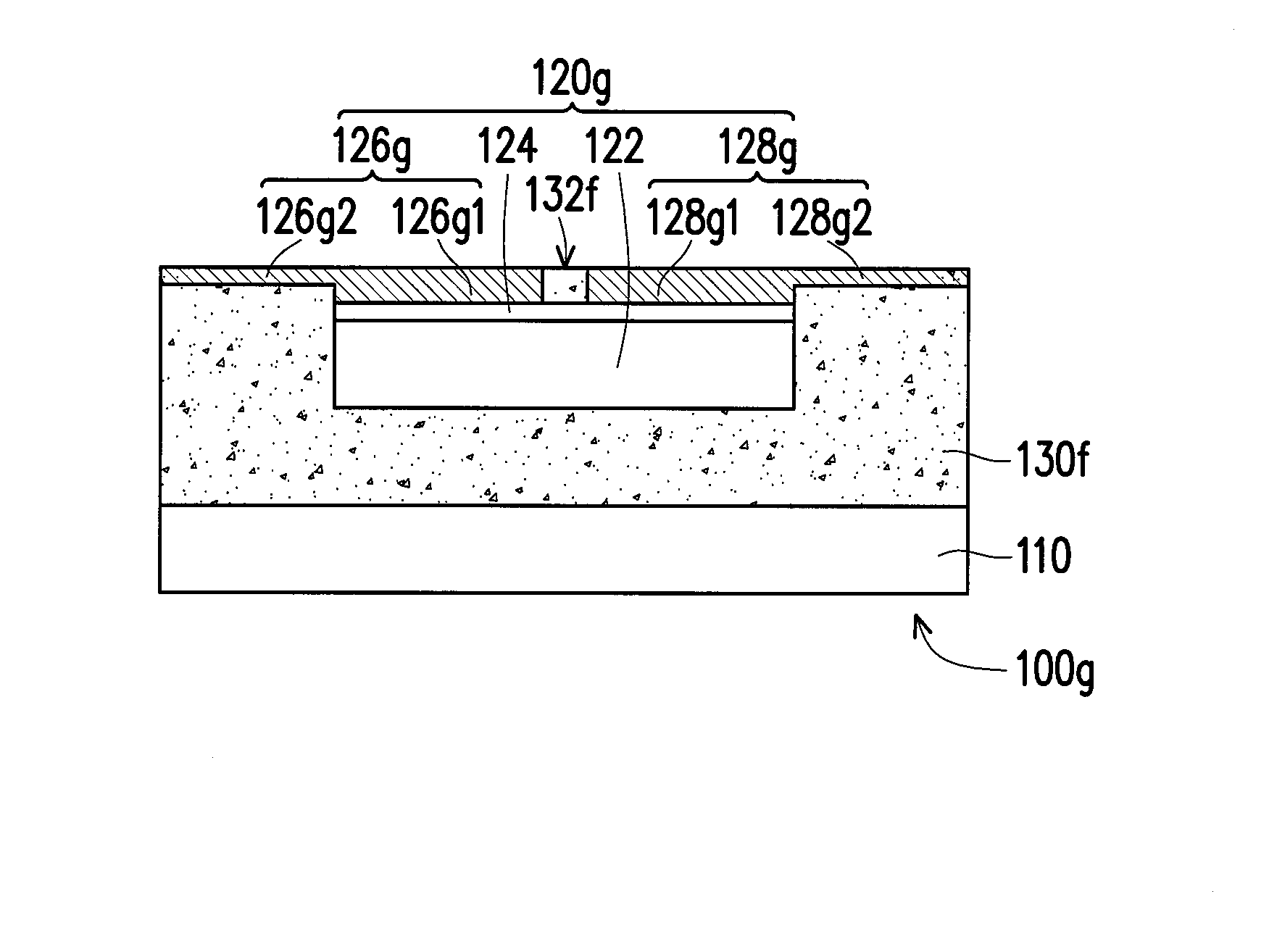
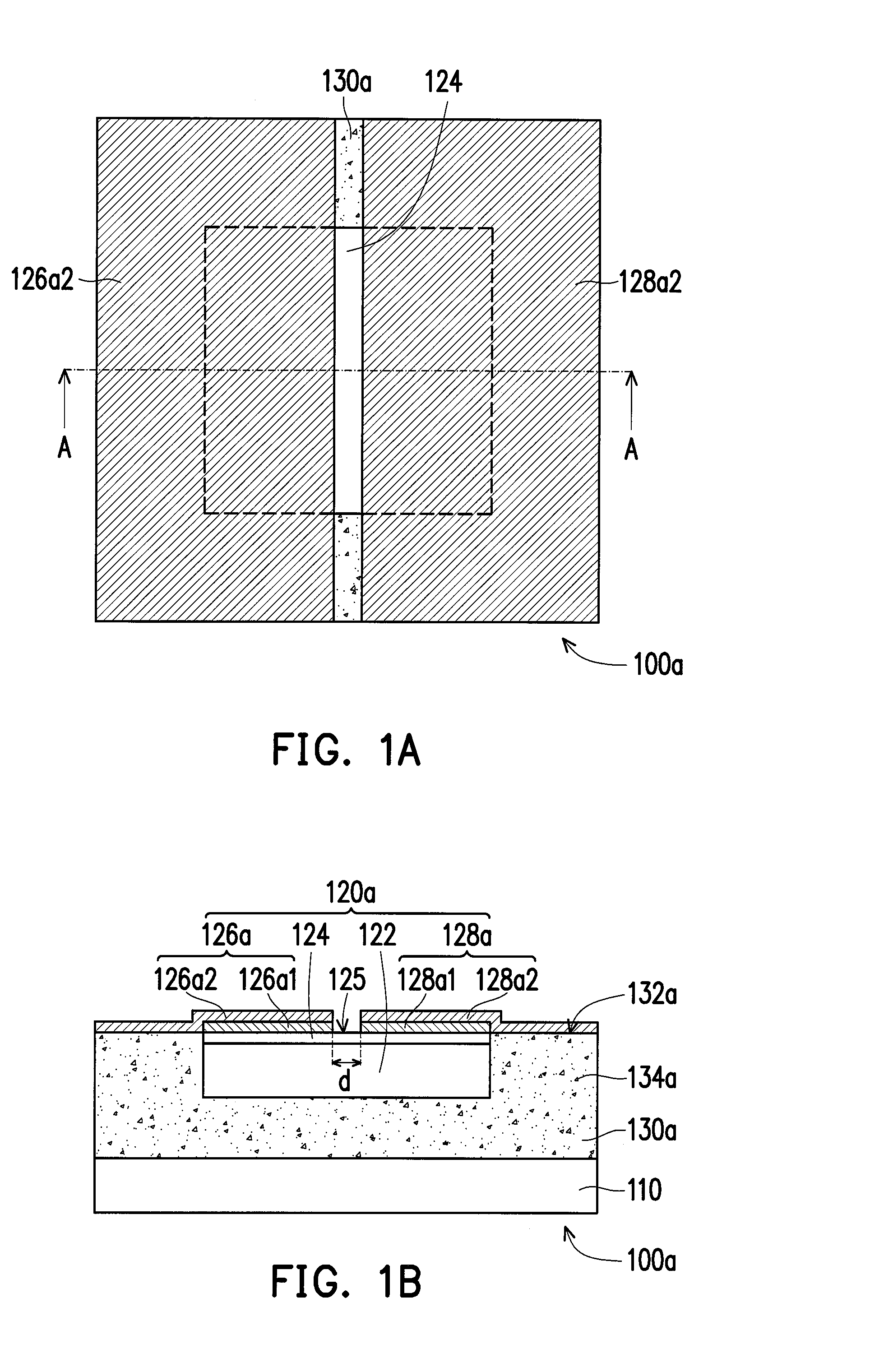
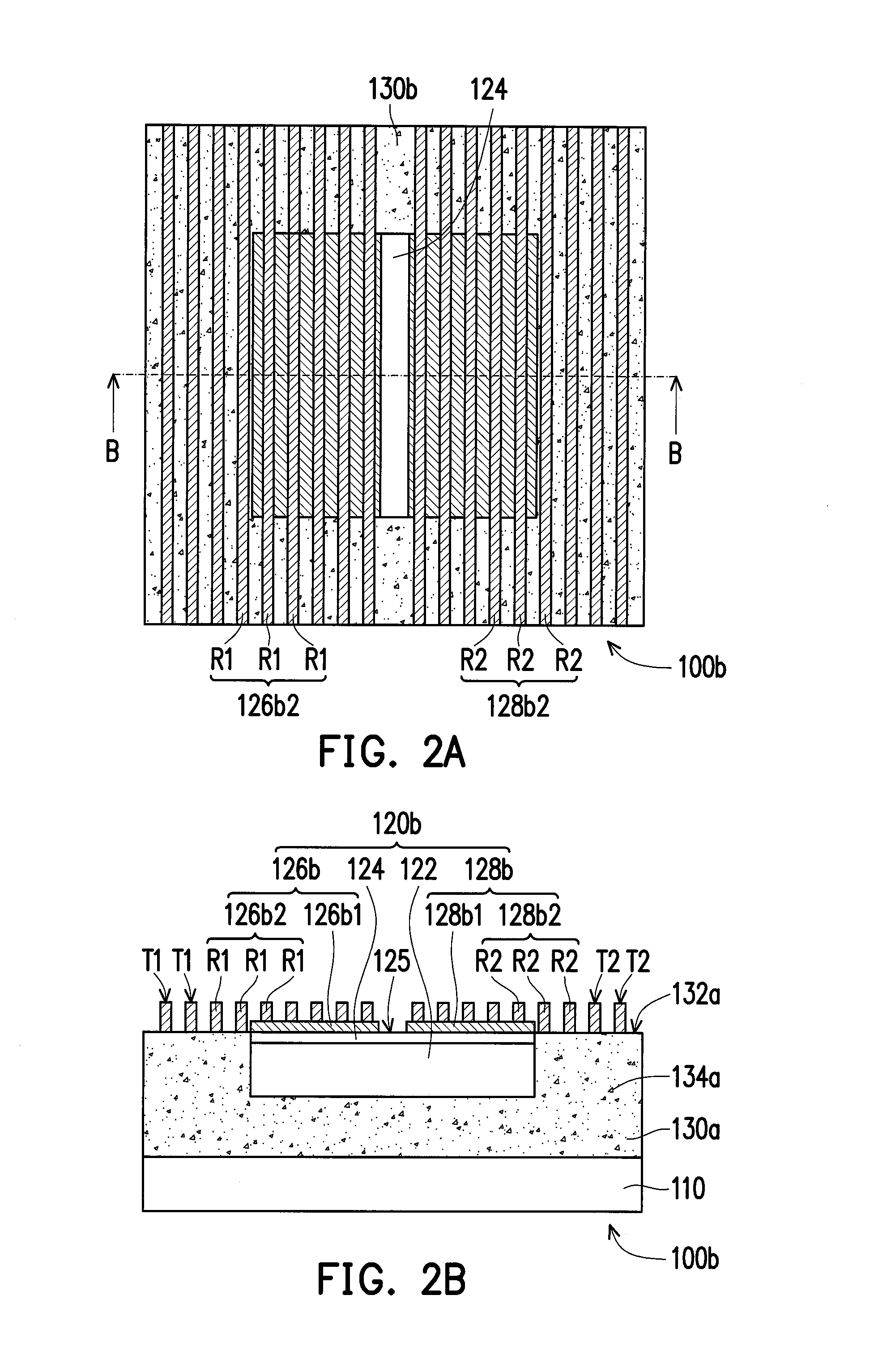
[0071]FIG. 1A is a top view of a light emitting device according to an embodiment of the invention. FIG. 1B is a cross-sectional view of the light emitting device of FIG. 1A viewing along a line A-A. Referring to FIG. 1A and FIG. 1B, in the present embodiment, the light emitting device 100a includes a light transmissive layer 110, a light emitting unit 120a, and an encapsulant 130a. The light emitting unit 120a is, for example, a light emitting diode (LED), and includes a substrate 122, an epitaxial structure layer 124, a first electrode 126a and a second electrode 128a. The epitaxial structural layer 124 is disposed on the substrate 122. In the present embodiment, a periphery of the epitaxial structure layer 124 is aligned with a periphery of the substrate 122. The first electrode 126a is disposed on one side of the epitaxial structure layer 124. The second electrode 128a is disposed on the epitaxial structure layer 124, where the second electrode 128a and the first electrode 126a ...


PUM


Abstract

A light emitting device includes a light emitting unit, a light transmissive layer and an encapsulant. The light emitting unit includes a substrate, an epitaxial structure layer disposed on the substrate, and a first electrode and a second electrode disposed on the same side of the epitaxial structure layer, respectively. The light emitting unit is disposed on the light transmissive layer and at least a part of the first electrode and a part of the second electrode are exposed by the light transmissive layer. The encapsulant encapsulates the light emitting unit and at least exposes a part of the first electrode and a part of the second electrode. Each of the first electrode and the second electrode extends outward from the epitaxial structure layer, and covers at least a part of an upper surface of the encapsulant, respectively.

Description

CROSS-REFERENCE TO RELATED APPLICATION[0001]This application claims the priority benefits of Taiwan application serial no. 103116262, filed on May 7, 2014, Taiwan application serial no. 104113482, filed on Apr. 27, 2015, and Taiwan application serial no. 103116987, filed on May 14, 2014. The entirety of each of the above-mentioned patent applications is hereby incorporated by reference herein and made a part of this specification.BACKGROUND OF THE INVENTION[0002]1. Field of the Invention[0003]The invention relates to a light emitting device, and particularly relates to a light emitting diode (LED) package structure.[0004]2. Description of Related Art[0005]In a conventional flip-chip LED package structure, an edge of an epitaxial structure layer is aligned with or contracted inward relative to an edge of a substrate, and edges of an N electrode and a P electrode are aligned with the edge of the epitaxial structure layer or is spaced by a vertical distance with the edge of the epitaxi...

Claims


Application Information

Patent Timeline
IPC IPC(8): H01L33/38H01L33/50H01L33/60H01L33/40H01L33/52
CPCH01L33/38H01L33/40H01L33/502H01L33/60H01L33/52H01L33/62H01L33/46H01L33/54H01L33/486H01L33/56
Inventor TING, SHAO-YINGHUANG, KUAN-CHIEHHUANG, JING-ENLIN, YU-FENGHUANG, YI-RU
Owner GENESIS PHOTONICS
Learn More