Printed Circuit Board

a technology of printed circuit boards and circuit boards, which is applied in the direction of printed circuit aspects, printed circuit non-printed electric components association, electrical apparatus, etc., can solve the problems of increased costs, increased pcb overall height (or thickness), and serious problems with signal integrity in pcbs

Inactive Publication Date: 2015-11-19
AT & S AUSTRIA TECH & SYSTTECHN AG
View PDF13 Cites 8 Cited by
  • Summary
  • Abstract
  • Description
  • Claims
  • Application Information

AI Technical Summary

Benefits of technology

[0007]An object of the present invention is to provide a multilayer PCB with components even of different dimensions, without an undue increase of the total height of the PCB.

Problems solved by technology

Increasing miniaturization and extreme electronic component density as well as the necessity to transfer large amounts of data at high speed, e.g. at rates of 1 to 5 Gbps, can create serious problems with respect to signal integrity in PCBs.
The need to embed chips in a supplementary package leads not only to additional costs but also to an increase in overall height (or thickness) of the PCBs.

Method used


Image

  • Printed Circuit Board
  • Printed Circuit Board

Examples


Embodiment Construction

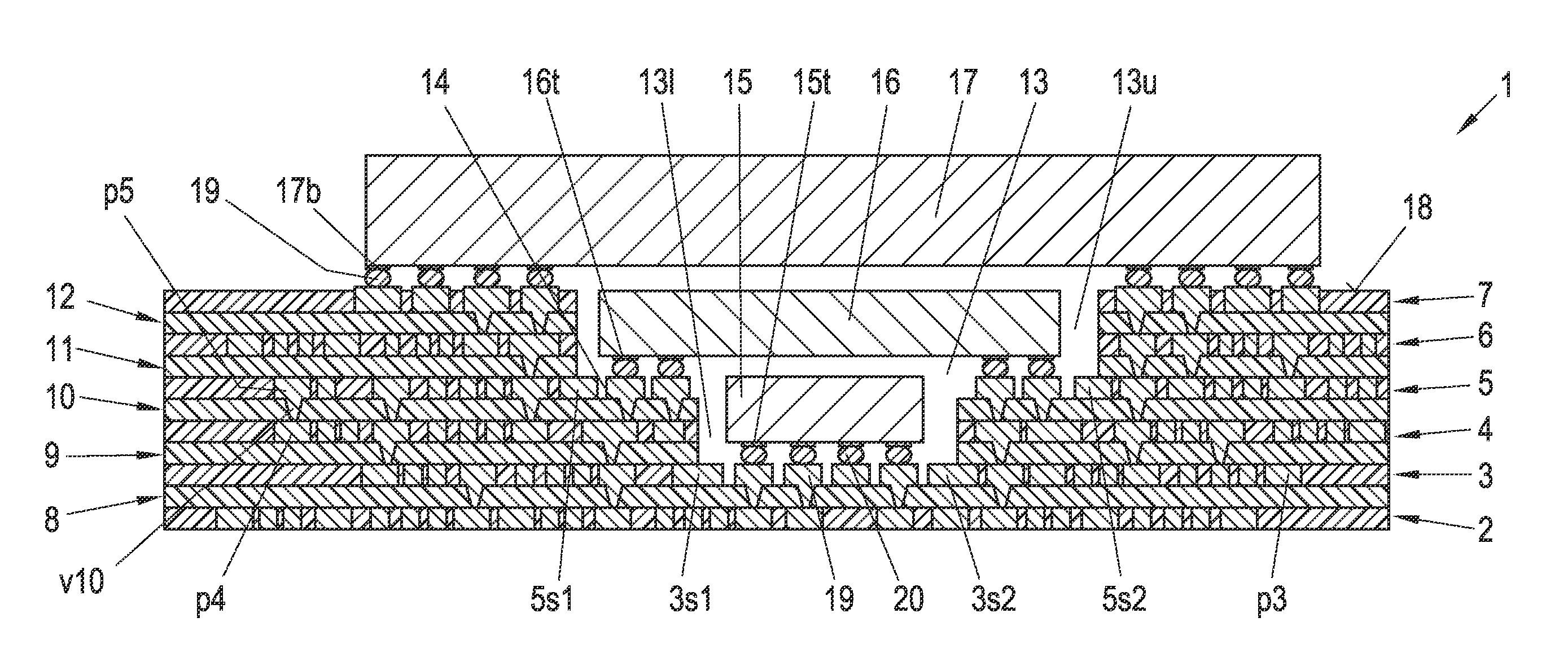
[0021]Embodiments of a PCB according to the invention will be described below in more detail with reference to the accompanying drawings. For same or similar components same reference numerals are used in order to avoid redundant explanations.

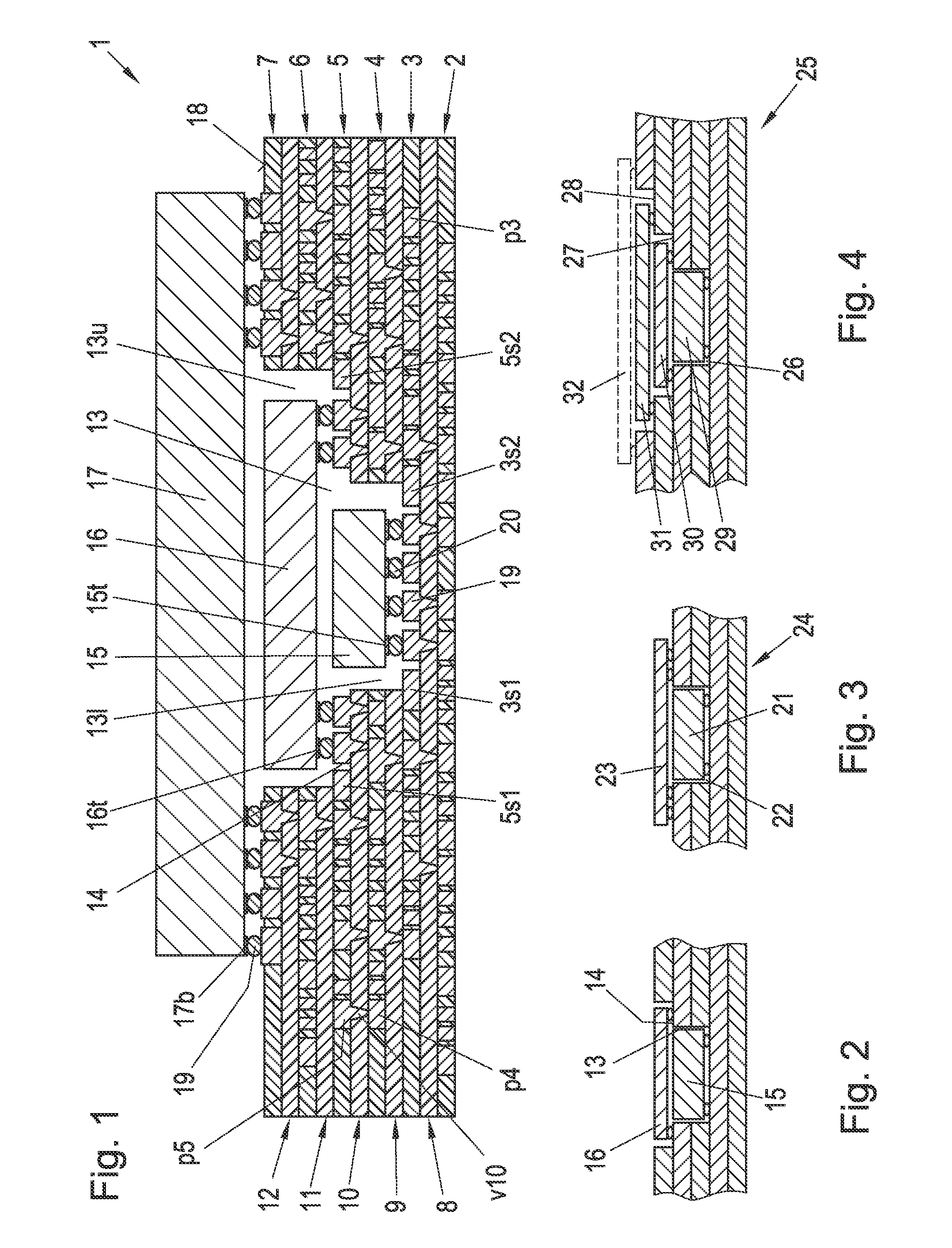
[0022]A printed multilayer circuit board 1 with a HDI-structure according to the invention, as shown in FIG. 1, comprises six structured conducting layers of conductive material like copper, the conducting layer designated from bottom to top with reference numerals 2, 3, 4, 5, 6 and 7, the conducting layers being separated by dielectric insulation layers 8, 9, 11 and 12. It can be seen that the conducting layers include a plurality of conducting paths, such as for example p3 in layer 3. Several conducting paths of different layers are connected by conducting vias. As for example conducting paths p4 and p5 are interconnected by a via v10, passing insolating layer 10.

[0023]In the circuit board 1 at least one cavity 13 is formed. In this example c...


PUM


Abstract

A multilayer printed circuit board comprising conductive layers separated by dielectric insulation layers, at least one conductive layer being patterned and parts of conducting layers being interconnected by means of vias traversing insulation layers, and at least one component having terminals electrically connected with conducting layers is countersunk at least partly in a cavity having a floor and side walls, whereby a first component is completely countersunk in the cavity with its terminals connected face-down directly with contacts on the floor of the cavity and at least one further component is stacked above the first component, whereby an edge of the lower surface of the second component projecting over the upper surface area of the at least one further component is provided with terminals being connected directly face-down with contacts of the circuit board arranged on a level higher than the floor of the cavity.

Description

BACKGROUND OF THE INVENTION[0001]1. Field of the Invention[0002]The present invention relates to a printed circuit board (PCB) and in particular to a multilayer printed circuit board comprising conductive layers separated by dielectric insulation layers, at least one conductive layer being patterned and parts of conducting layers being interconnected by means of vias traversing insulation layers, and at least one component having terminals electrically connected with conducting layers is countersunk at least partly in a cavity having a floor and side walls.[0003]2. Description of the Related Art[0004]Increasing miniaturization and extreme electronic component density as well as the necessity to transfer large amounts of data at high speed, e.g. at rates of 1 to 5 Gbps, can create serious problems with respect to signal integrity in PCBs. Accordingly it is desirable to have short and direct signal lines between components. The demand to produce HDI-PCBs (HDI is a broadly used acronym...

Claims


Application Information

Patent Timeline
Patent Type & Authority Applications(United States)
IPC IPC(8): H05K1/18H05K1/02H05K1/11
CPCH05K1/183H05K1/115H05K2201/10515H05K1/0298H05K2201/09036H05K1/181H01L2224/16227H01L2924/15156H05K3/4697H05K2201/09072H05K2201/09845H05K2201/10727H05K2201/10734
Inventor SCHMID, GERHARD
Owner AT & S AUSTRIA TECH & SYSTTECHN AG
Why Eureka
Try Eureka