
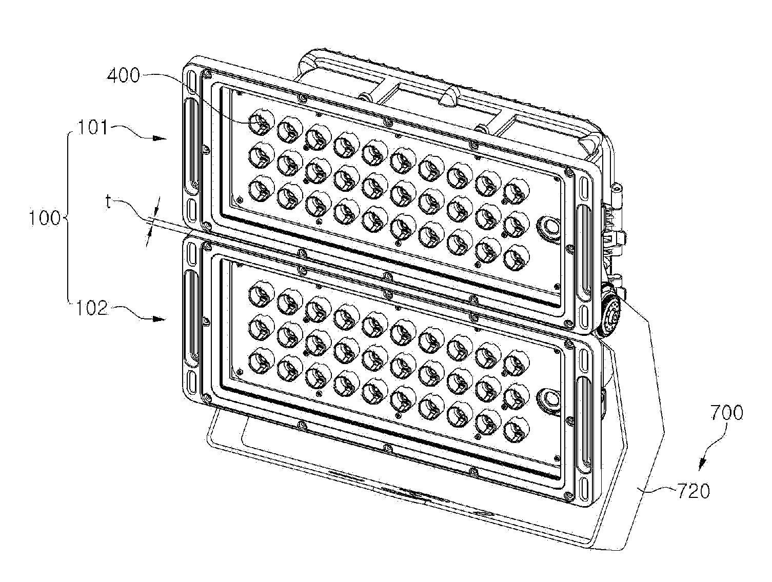
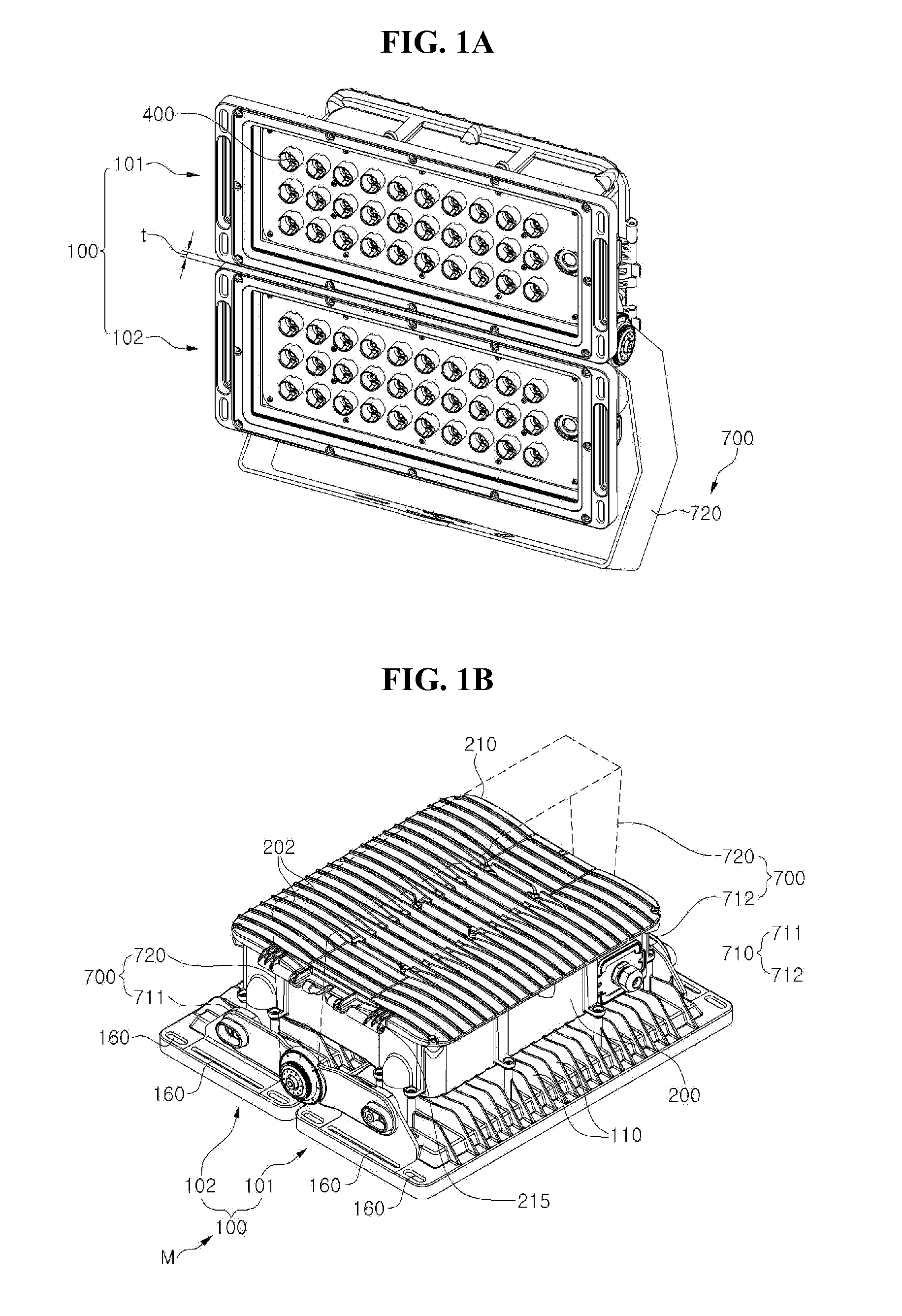
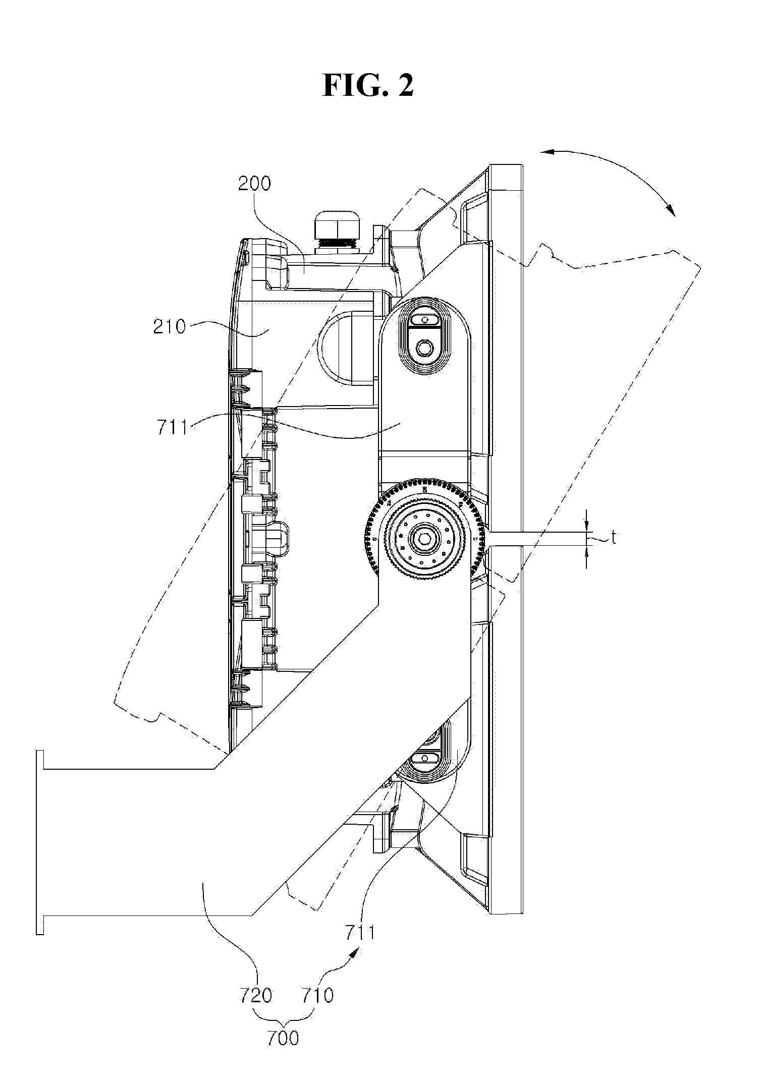
Optical semiconductor illuminating apparatus

a technology of optical semiconductors and illumination apparatuses, applied in the direction of lighting and heating apparatus, semiconductor devices for light sources, planar light sources, etc., can solve the problems of cumbersome and inconvenient, increase and decrease of light flux or light quantity depending on installation and construction environment,

Inactive Publication Date: 2015-12-03
GLOW ONE CO LTD
View PDF4 Cites 11 Cited by
  • Summary
  • Abstract
  • Description
  • Claims
  • Application Information

AI Technical Summary

Benefits of technology

The present invention is an optical semiconductor illuminating apparatus that improves heat dissipation performance by inducing natural convection across inner and outer portions of the apparatus. It is simple to install and constructed and actively takes action against various construction environments such as expansion and reduction due to assembling and fastening. Additionally, it can maintain waterproofing and airtightness and improve workability even in a case of maintenance such as a repair, a replacement, and the like. The apparatus includes a light emitting module including semiconductor optical elements, a casing part having a switching mode power supply (SMPS) embedded therein, a first airtightness part including a packing frame fixed to an outer side of an edge of a communication slot penetrating through a side surface of the casing part, and a second airtightness part provided to an upper side of the casing part to prevent water and foreign materials from being introduced from the outside.

Problems solved by technology

Particularly, since a light emitting module connected to the heat sink generally has a constant light flux or quantity of light depending on an area thereof or the number of optical semiconductors, there was a problem that an increase and decrease in the light flux or the quantity of light depending on an installation and construction environment is itself impossible.
However, since the cable gland has the cable which is directly connected up to an inner portion of the housing, it is cumbersome and inconvenient in that the entire housing needs to be separated and opened to check the inner portion of the housing when it is determined that a terminal connecting part of the cable is abnormal.

Method used


Image

  • Optical semiconductor illuminating apparatus
  • Optical semiconductor illuminating apparatus
  • Optical semiconductor illuminating apparatus

Examples


Embodiment Construction

[0029]Advantages and features of the present invention and methods accomplishing them will become apparent from the following description of exemplary embodiments with reference to the accompanying drawings.

[0030]However, the present invention may be modified in many different forms and it should not be limited to exemplary embodiments set forth herein.

[0031]These exemplary embodiments may be provided so that this disclosure will be thorough and complete, and will fully convey the scope of the invention to those skilled in the art.

[0032]In addition, the present invention is defined solely by the scope of the claims.

[0033]Therefore, in some exemplary embodiments, components, operations, and technologies which are widely known are not described in detail in order to avoid obscuring the disclosed subject matter.

[0034]In addition, like reference numerals throughout the specification denote like element, and terms used (referred) in the present specification are for explaining the exempl...


PUM


Abstract

An optical semiconductor illuminating apparatus includes a light emitting module including semiconductor optical elements, a casing part disposed over the light emitting module and having a switching mode power supply (SMPS) embedded therein, a first airtightness part including a packing frame fixed to an outer side of an edge of a communication slot penetrating through a side surface of the casing part, and a second airtightness part provided to an upper side of the casing part.

Description

CROSS-REFERENCE TO RELATED APPLICATIONS[0001]This application claims priority from and the benefit of Korean Patent Application No. 10-2014-0065362, filed on May 29, 2014, and Korean Patent Application No. 10-2014-0065363, filed on May 29, 2014, which are hereby incorporated by reference for all purposes as if fully set forth herein.BACKGROUND[0002]1. Field[0003]The present invention relates to an optical semiconductor illuminating apparatus.[0004]2. Discussion of the Background[0005]An optical semiconductor such as a light emitting diode (LED) or a laser diode (LD) is one of the components that have been recently spotlighted widely as an illuminating apparatus due to lower power consumption, a longer lifespan, more excellent durability, and significantly higher brightness as compared with an incandescent lamp and a fluorescent lamp.[0006]Typically, since heating is inevitably caused from the optical semiconductor in an illuminating fixture using the optical semiconductor described ...

Claims


Application Information

Patent Timeline
IPC IPC(8): F21V31/00F21V17/12F21V23/00
CPCF21V31/005F21V23/001F21Y2101/025F21V17/12F21Y2101/02F21V23/007F21V15/013F21V23/008F21V29/763F21V29/83F21Y2105/10F21Y2115/10
Inventor KANG, SEOK JINJANG, YOON GILKIM, SANG HYUKPARK, IILEE, SU WOONJEONG, MIN A.
Owner GLOW ONE CO LTD
Learn More