Light emitting display panel and manufacturing method thereof

a technology of light-emitting display panels and manufacturing methods, applied in the field of electronic components, can solve the problems of increasing the area of non-luminous regions, damage to the oled layer, and the inability to manufacture large-size oled devices, so as to increase the effect of preventing water vapor and prolonging the invasion path of water vapor

Active Publication Date: 2015-12-03
BOE TECH GRP CO LTD
View PDF17 Cites 21 Cited by
  • Summary
  • Abstract
  • Description
  • Claims
  • Application Information

AI Technical Summary

Benefits of technology

[0006]To this end, embodiments of the present invention provide a light emitting display panel in order to prolong an invasion path of the water vapor and oxygen gas and to increase an effect of preventing the water vapor and oxygen gas, lifetime of the OLED devices is thus prolonged.
[0040]Embodiments of the present invention achieve an effect of prolonging an invasion path of the water vapor and oxygen gas spatially and thus increasing an effect of preventing the water vapor and oxygen gas by forming at least two rows of protruded frames on a cover plate of liquid crystal display panel and forming a row of protruded frame on a substrate correspondingly which can be embedded between the at least two rows of protruded frames on the cover plate and by filling resin adhesive or desiccant in gaps between these frames.

Problems solved by technology

However, water vapor and oxygen gas would permeate into the OLED devices through the packaging adhesive when only the resin adhesive is used to package.
In addition, a distance from an outer edge of the adhesive to OLED is typically increased in order to improve an effect of preventing water vapor and oxygen gas, but widening a region of adhesive may only be conducted in a plane in the traditional OLED substrate and cover plate, thereby this will increase an area of non-luminous region, which is disadvantaged to realize a manufacture of narrow bezel display panel.
However, laser is needed during curing the glass cement and it may damage the OLED layer.
Moreover, if only the glass cement is used to package the OLED devices, manufacture of large-size OLED devices cannot be achieved because a glass plate would collapse in its central portion.

Method used


Image

  • Light emitting display panel and manufacturing method thereof
  • Light emitting display panel and manufacturing method thereof
  • Light emitting display panel and manufacturing method thereof

Examples


Embodiment Construction

[0046]In order to make objectives, technical solutions and advantages of the embodiments of the invention more clear and apparent, hereinafter, the technical solutions of the invention will be described in detail in connection with the specific embodiments and referring to the accompanying drawings.

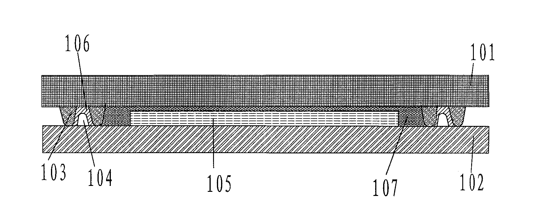
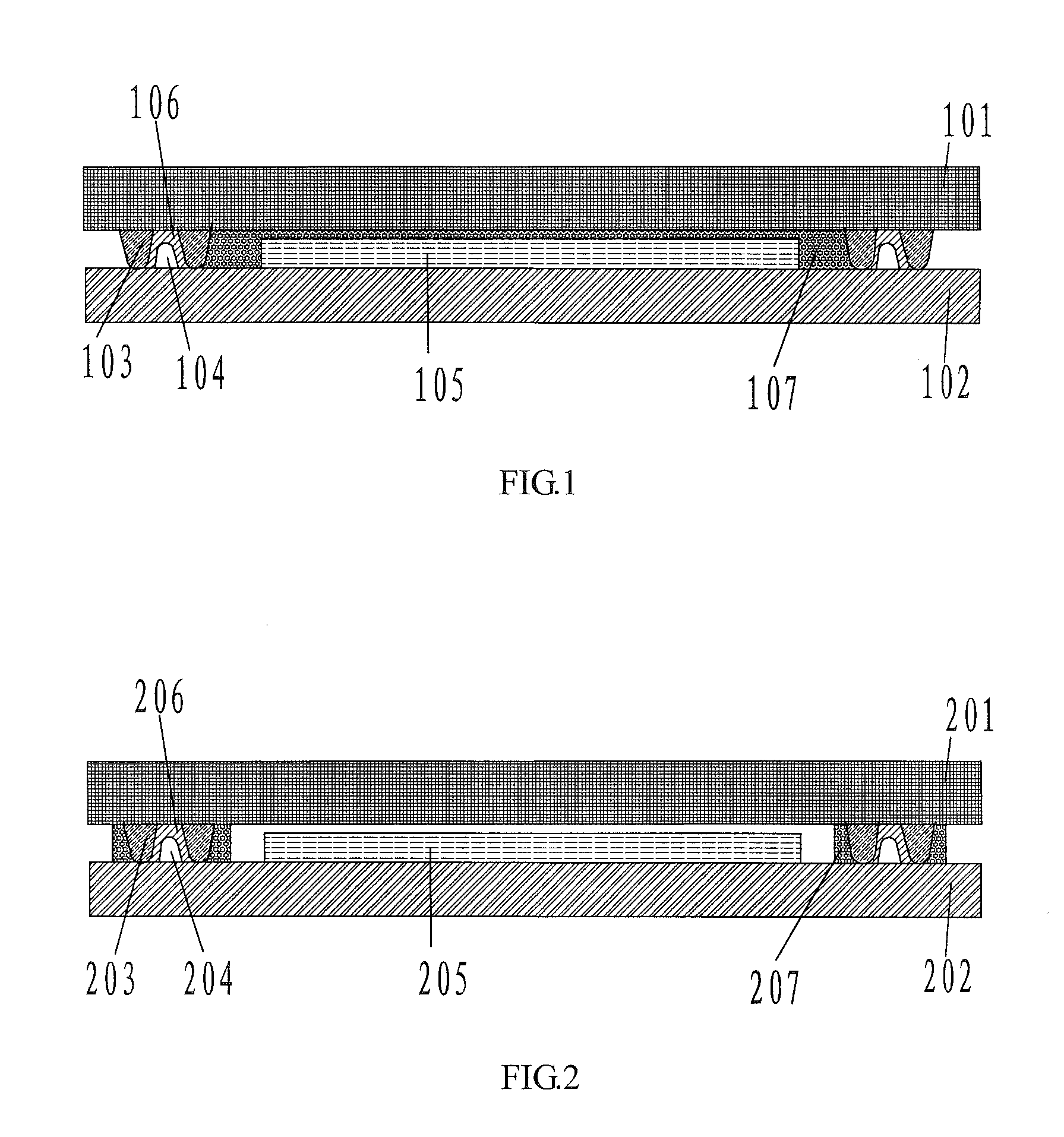
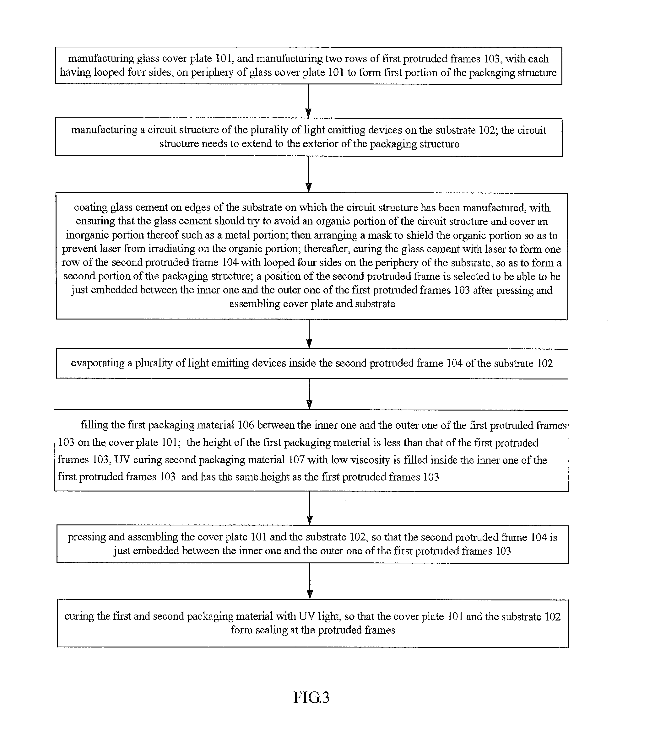
[0047]Embodiments of the invention provide a light emitting display panel. The light emitting display panel comprises a cover plate and a substrate disposed opposite to each other, a plurality of light emitting devices located between the cover plate and the substrate, and a packaging structure surrounding the light emitting devices. The packaging structure comprises at least three rows of protruded frames and a first packaging material which is located between adjacent protruded frames, wherein four sides of each of the protruded frames are looped and the at least three rows of protruded frames are adjacent to and embedded in each other in an inward and outward direction. Adjacent ones o...


PUM


Abstract

Embodiments of the invention disclose a light emitting display panel. The light emitting display panel comprises a cover plate, a substrate disposed opposite to each other, a plurality of light emitting devices located between the cover plate and the substrate, and a packaging structure surrounding the light emitting devices. The packaging structure comprises at least three rows of protruded frames and a first packaging material which is located between adjacent protruded frames, wherein four sides of each of the protruded frames are looped and the at least three rows of protruded frames are adjacent to and embedded in each other in an inward and outward direction. Adjacent ones of the at least three rows of protruded frames are alternately disposed on the cover plate and the substrate and protrude in opposite directions, and non-adjacent ones of the at least three rows of protruded frames are disposed on the same one of the cover plate and the substrate and protrude in the same direction. In the above light emitting display panel, resin adhesive or desiccant is filled in gaps between the frames so as to prolong an invasion path of water vapor and oxygen gas spatially, an effect of preventing water vapor and oxygen gas is thus increased. The light emitting display panel has advantages of good sealing property, simple manufacturing process and the like.

Description

BACKGROUND OF THE INVENTION[0001]1. Field of the Invention[0002]Embodiments of the present invention relate to a technical field of electronic components, in particular, to a light emitting display panel and a manufacturing method thereof.[0003]2. Description of the Related Art[0004]An OLED device refers to such an electroluminescent device that is formed of an organic semiconductor material and a luminous material and is caused to emit light through injection and recombination of carriers upon it being driven by an electric field. OLED devices have many advantages and possess bright prospects in the field of display. OLED devices are very sensitive to water vapor and oxygen gas, and water vapor and oxygen gas that permeate into OLED devices are main factors that affect lifetime of the OLED devices. Thus, OLED devices are usually packaged by a packaging structure so as to prevent the water vapor and oxygen gas permeating.[0005]In the prior art, a common packaging structure is to pac...

Claims


Application Information

Patent Timeline
Patent Type & Authority Applications(United States)
IPC IPC(8): H01L51/52H01L51/56
CPCH01L51/5237H01L51/5246H01L2227/323H01L51/56H01L51/5259H10K50/846H10K50/8426H10K50/8428H10K50/84H10K71/00H10K59/1201
Inventor LUO, CHENGYUANWANG, CHUN-JAN
Owner BOE TECH GRP CO LTD
Why Eureka
Try Eureka