OLED panel for lighting device

a technology of light-emitting diodes and lighting devices, which is applied in the direction of semiconductor devices for light sources, lighting and heating apparatus, electroluminescent light sources, etc., can solve the problems of environmental problems, low color rendering index, and very low energy efficiency, and achieve the effect of preventing the degradation of the oled emission structure due to external moisture intrusion and reducing the delay effect of high moisture intrusion

Active Publication Date: 2019-06-20
LG DISPLAY CO LTD
View PDF3 Cites 0 Cited by
  • Summary
  • Abstract
  • Description
  • Claims
  • Application Information

AI Technical Summary

Benefits of technology

[0023]Through the groove penetrating through the passivation pattern arranged in the dummy area of the substrate, the lower surface of the adhesive layer in the dummy area may have a 3D structure. Accordingly, the path along which moisture intrudes may be increased, and thus degradation of the OLED emission structure due to external moisture intrusion may be prevented. Furthermore, the passivation pattern between the grooves may act as a barrier to the moisture intrusion.
[0024]Preferably, the groove may further penetrate through the first electrode and the auxiliary wiring pattern arranged under the passivation pattern in the dummy area of the substrate. Furthermore, the side wall of the groove may have a step shape. Since the height and the step-shaped structure of the groove may further increase the path of the moisture intrusion, high moisture intrusion delay effect may be obtained.

Problems solved by technology

For incandescent lamps, a color rendering index is high, but energy efficiency is very low.
For fluorescent lamps, while energy efficiency is high, a color rendering index is low.
Furthermore, since a fluorescent lamp contains mercury, an environmental problem occurs.
Accordingly, when a white light is emitted by combining a red emission diode, a green emission diode, and a blue emission diode, the emission efficiency may deteriorate.
Furthermore, when a red emission diode, a green emission diode, and a blue emission diode are in use, color rendering characteristics may deteriorate because the width of an emission peak of each diode is narrow.
However, in the lighting device that outputs a white light by combining a blue emission diode and a yellow phosphor, the phosphor substance for emitting a yellow light has poor emission efficiency.
Thus, there has been a limitation in improving the emission efficiency of a lighting device.
Furthermore, for high-quality growth of nitride semiconductor, an expensive sapphire substrate is used.
Furthermore, not much heat is generated compared to the nitride semiconductor light-emitting diode.
However, in an OLED based lighting device, an OLED is vulnerable to moisture.
As the intrusion of moisture continues in the OLED, the OLED may deteriorate and light emission performance may be degraded.
Accordingly, the life characteristics of a lighting device may deteriorate.

Method used


Image

  • OLED panel for lighting device
  • OLED panel for lighting device
  • OLED panel for lighting device

Examples


Embodiment Construction

[0038]Hereinafter, an OLED panel for a lighting device according to embodiments of the present disclosure, and a manufacturing method thereof, will be described in detail with reference to the accompanying drawings.

[0039]Terms such as “first” and “second” are used herein merely to describe a variety of constituent elements, but the constituent elements are not limited by the terms. Such terms are used only for the purpose of distinguishing one constituent element from another constituent element.

[0040]Furthermore, in the present disclosure, when a constituent element is disposed “above” or “on” to another constituent element, the constituent element may be not only directly on the other constituent element, but also above the other constituent element in a non-contact manner through at least one of other constituent elements, e.g., a third constituent element.

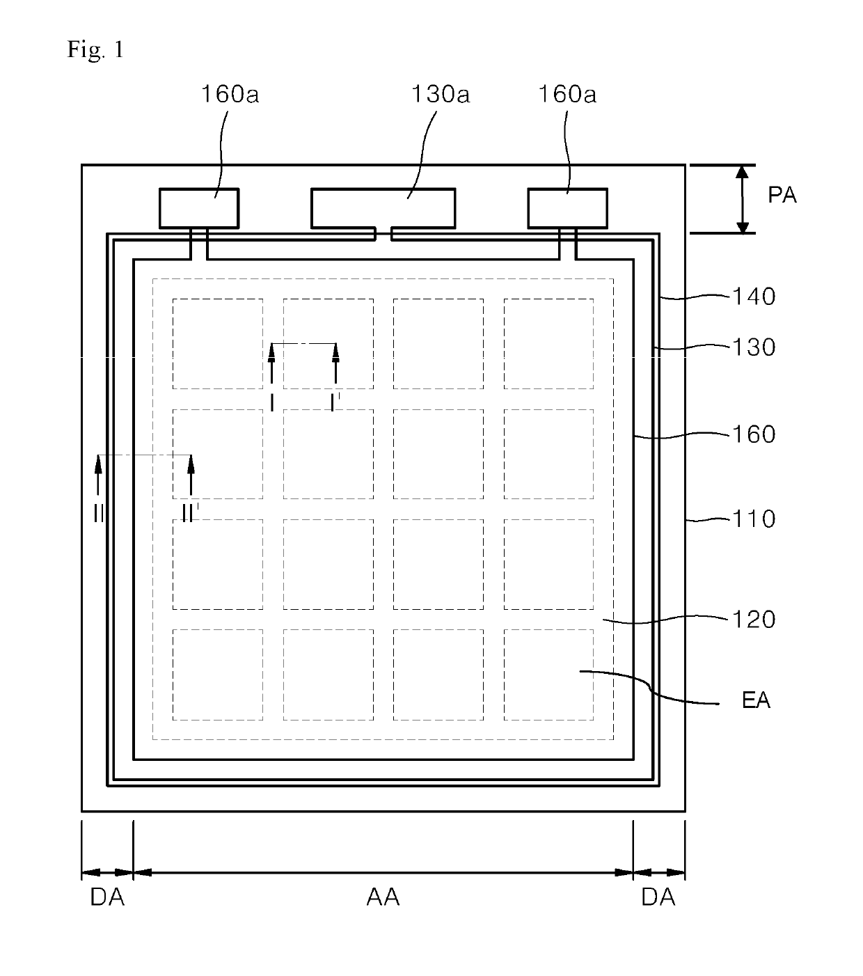
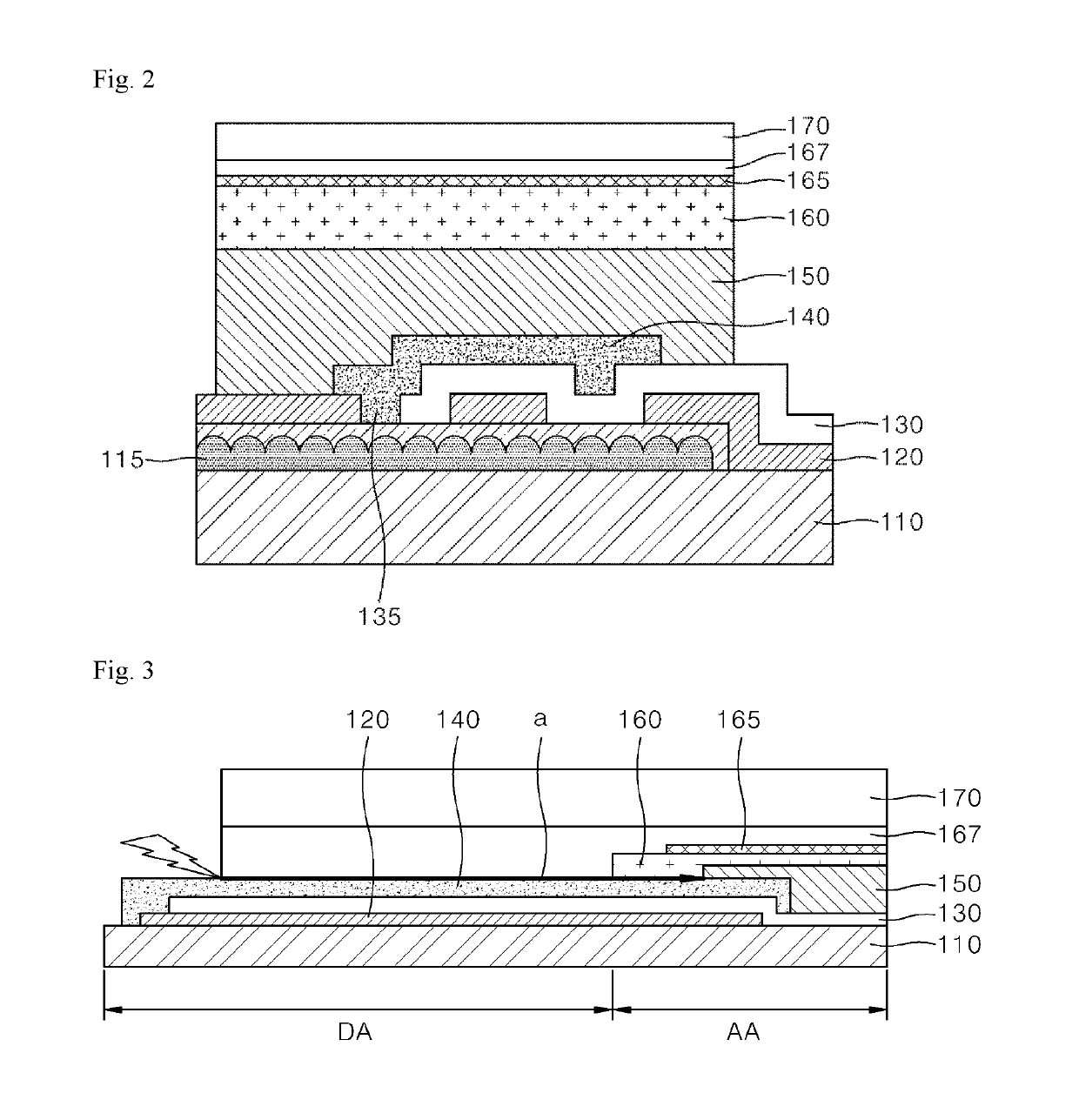
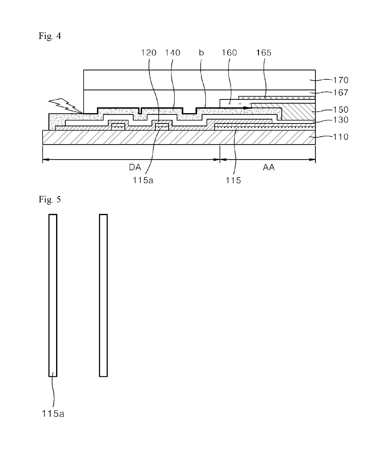
[0041]FIG. 1 is a schematic plan view of an OLED panel for a lighting device according to an embodiment of the present disclo...


PUM


Abstract

An organic light-emitting diode panel for a lighting device includes a substrate including an array area having an emission area and a dummy area disposed outside the array area, an auxiliary wiring pattern, a first electrode, a passivation pattern, an OLED emission structure, a second electrode, an adhesive layer, and an encapsulation layer. The passivation pattern and the adhesive layer have an uneven boundary surface therebetween in the dummy area. Alternatively, a lower surface of the adhesive layer has a 3D structure. Thus, a moisture intrusion path between the passivation pattern and the adhesive layer of the dummy area of the substrate may be increased. Thus, degradation of the OLED emission structure due to external moisture intrusion may be reduced or prevented.

Description

CROSS-REFERENCE TO RELATED APPLICATION[0001]This application claims priority under 35 U.S.C. § 119 to Korean Application No. 10-2017-0172831, filed on Dec. 15, 2017, whose entire disclosure is herein incorporated by reference.BACKGROUNDTechnical Field[0002]The present disclosure relates to a light-emitting panel for a lighting device, and more particularly, to an organic light-emitting diode (OLED) panel having an excellent moisture intrusion delay effect and excellent life characteristics.Description of the Related Art[0003]Fluorescent lamps or incandescent lamps are mainly used as lighting devices. For incandescent lamps, a color rendering index is high, but energy efficiency is very low. For fluorescent lamps, while energy efficiency is high, a color rendering index is low. Furthermore, since a fluorescent lamp contains mercury, an environmental problem occurs.[0004]Recently, light-emitting diode (LED) based lighting devices have been suggested. LEDs are formed in a stack structu...

Claims


Application Information

Patent Timeline
Patent Type & Authority Applications(United States)
IPC IPC(8): H01L51/52H01L27/32
CPCH01L51/5253H01L27/3213H01L27/3223H10K59/1315H10K59/131H10K50/00H10K50/805H10K50/84H10K59/88H10K50/814H10K50/8426H10K50/844H05B33/04F21Y2115/15H10K50/85H10K59/351
Inventor KIM, TAEOKLEE, SHIN-BOK
Owner LG DISPLAY CO LTD
Why Eureka
Try Eureka