Device for manufacturing a silicon structure, and manufacturing method thereof

a manufacturing method and silicon technology, applied in the direction of microstructural devices, microstructure devices, coatings, etc., can solve the problems of structure essentially failing to function as a sensor, actuator, etc., and the manufacturing process of the structure becomes complicated

Inactive Publication Date: 2008-10-23
TOYOTA CENT RES & DEV LAB INC
View PDF42 Cites 57 Cited by
  • Summary
  • Abstract
  • Description
  • Claims
  • Application Information

AI Technical Summary

Benefits of technology

[0018]Sensors, actuators, and the like require a high degree of sensitivity and accuracy. In order to fulfill these requirements, the tendency is to reduce the rigidity of the structure and to miniaturize the size of the structure. However, the likelihood of the sticking phenomenon occurring as a result of wet etching increases when the rigidity of the structure is reduced or the size of the structure is miniaturized. Consequently, the number of defective articles produced as a result of wet etching has increased in recent years.
[0071]According to the above aspect, after dry etching of the silicon structure has been completed in the etching reaction chamber, the silicon structure can be conveyed to the coating chamber without its coming into contact with the outside air. As a result, oxidization etc. of the silicon structure can be prevented. Further, the provision of the preparatory chamber allows the silicon structure to be transferred easily between the etching reaction chamber and the coating chamber.

Problems solved by technology

Consequently, the manufacturing process for the structure becomes complicated.
Further, when wet etching is performed, there is a danger of an occurrence of the so-called sticking phenomenon.
If the sticking phenomenon occurs, the structure essentially fails to function as a sensor, actuator, etc.
That is, the sticking phenomenon creates defective articles, causing a drop in yield.
As a result, the structure essentially fails to function as an acceleration sensor.
As a result, the structure essentially fails to function as a pressure sensor.

Method used


Image

  • Device for manufacturing a silicon structure, and manufacturing method thereof
  • Device for manufacturing a silicon structure, and manufacturing method thereof
  • Device for manufacturing a silicon structure, and manufacturing method thereof

Examples


first embodiment

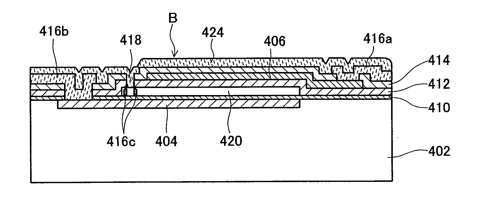
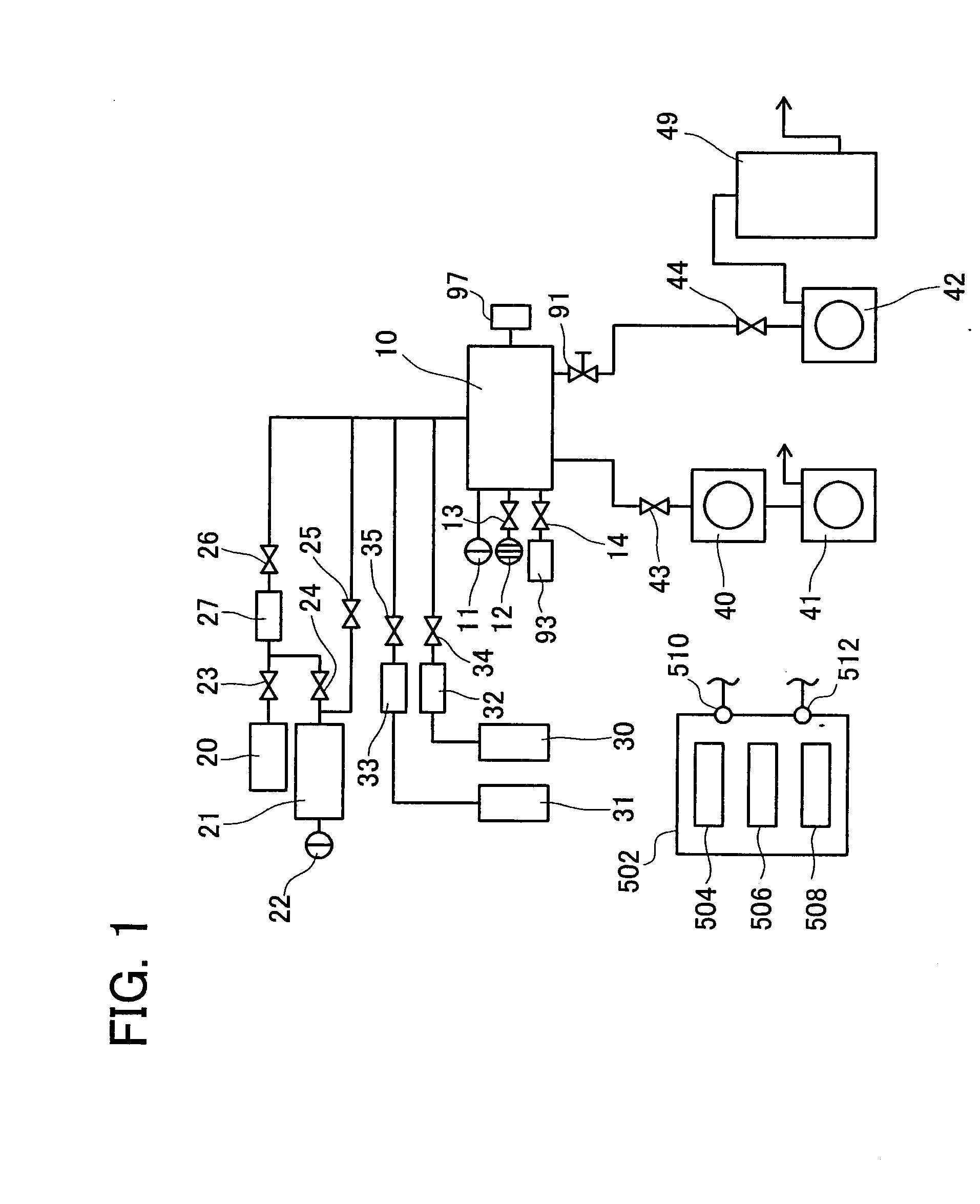
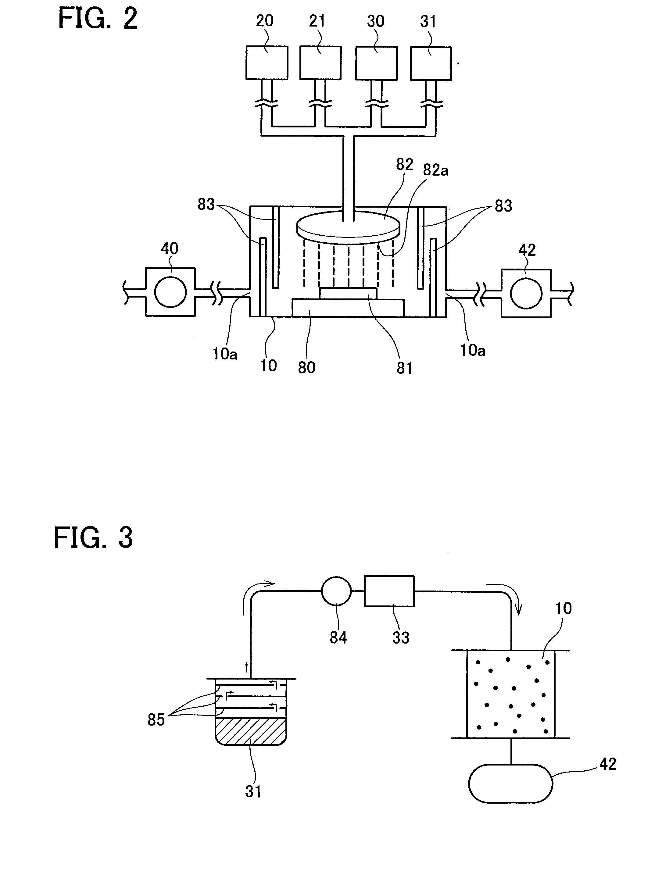
[0106]FIG. 1 shows the configuration of a device for manufacturing a silicon structure (hereafter referred to as ‘structure manufacturing device’) of a first embodiment. Since this device can be used for the entire processing of silicon material, it may equally well be referred to as a silicon material processing device. That is, the term ‘structure manufacturing device’ used below may equally well be replaced with ‘silicon material processing device.’

[0107]The structure manufacturing device of the first embodiment is provided with a xenon difluoride vessel 20, a sublimated gas storage vessel 21, a hydrogen fluoride vessel 30, a methyl alcohol vessel 31, an etching reaction chamber 10, a dry pump 42, a toxic substance removal device 49, a turbo-molecular pump 40, a rotary pump 41, and a control member 502, etc.

[0108]Solid xenon difluoride XeF2 is housed within the xenon difluoride vessel 20. The xenon difluoride is solid at regular temperature and at atmospheric pressure. Xenon difl...

second embodiment

[0165]FIG. 14 shows a structure of a device for manufacturing a silicon structure of a second embodiment. Descriptions are generally omitted below when content is identical with the first embodiment.

[0166]The structure manufacturing device of the second embodiment has the configurational elements of the structure manufacturing device of the first embodiment, and in addition thereto is provided with a coating chamber 50, an organosilicic compound vessel 60, a water vessel 61, etc.

[0167]Liquid organosilicic compound is housed within the organosilicic compound vessel 60. The liquid organosilicic compound may utilize, for example, tridecafluoro-1,1,2,2,-tetrahydrooctyl trichlorosilane (C8F13H4SiCl3), octadecyl trichlorosilane (C18H37SiCl3), etc. Water (H2O) is housed within the water vessel 61.

[0168]A third pressure meter 51 is connected with the coating chamber 50. A second vacuum meter 52 is connected with the coating chamber 50 via an eleventh valve 53. A nitrogen gas supply member 9...

third embodiment

[0176]FIG. 15 shows a configuration of a device for manufacturing a silicon structure of a third embodiment. Descriptions are generally omitted below when content is identical with the first and second embodiment.

[0177]The structure manufacturing device of the third embodiment has the configurational elements of the structure manufacturing device of the second embodiment, and in addition thereto is provided with a preparatory chamber 70, first and second connecting members 75 and 76, first and second opening and closing means 98 and 99, a silicon structure conveying means 96, etc.

[0178]The first connecting member 75 connects the etching reaction chamber 10 with the preparatory chamber 70 in a manner whereby space therebetween is isolated from the outside air. The second connecting member 76 connects the preparatory chamber 70 with a coating chamber 50 in a manner whereby space therebetween is isolated from the outside air.

[0179]The first opening and closing means 98 is capable of sw...


PUM

PropertyMeasurementUnit
pressureaaaaaaaaaa
microstructureaaaaaaaaaa
massaaaaaaaaaa

Abstract

A process for manufacturing a hollow silicon structure is simplified. A device for manufacturing the silicon structure is a device that manufactures the hollow silicon structure by processing a silicon structure, the silicon structure consisting of a silicon oxide layer formed on a silicon substrate, the silicon oxide layer being covered by a silicon layer. The device is provided with first gas supply members 20 and 21, second gas supply members 30 and 31, an etching reaction chamber 10, selective connecting means 23 to 26, 34 and 35, and a gas discharging means 42. The first gas etches silicon. The second gas etches silicon oxide and barely etches silicon. The selective connecting means 23 to 26, 34 and 35 selectively connect the etching reaction chamber 10 with either the first gas supply members 20 and 21 or the second gas supply members 30 and 31. The gas discharging means 42 discharges gas from the etching reaction chamber 10.

Description

CROSS-REFERENCE TO RELATED APPLICATION[0001]The present divisional application claims the benefit of priority under 35 U.S.C. § 120 to application Ser. No. 10 / 473,253, filed Sep. 29, 2003, which is the National Stage of PCT / JP02 / 02807, filed on Mar. 22, 2002, the both of which are incorporated herein by reference in their entirety. The present divisional application also claims the benefit of priority under 35 U.S.C. § 119 of Japanese Application No. 2001-096077, filed on Mar. 29, 2001, the entire contents of which are hereby incorporated herein by reference.FIELD OF THE INVENTION[0002]The present invention relates to a processing technique for silicon material and a manufacturing technique for a silicon structure. The silicon material of the present specification is monocrystal silicon, polycrystal silicon, silicon oxide, silicon nitride, etc. The silicon structure is a structure wherein silicon material is incorporated during or after manufacture. Materials other than the silicon ...

Claims


Application Information

Patent Timeline
Patent Type & Authority Applications(United States)
IPC IPC(8): H01L21/306B81B3/00B81C1/00H01L21/00
CPCH01L21/3065H01L21/31116H01L21/32135H01L21/67069H01L21/302
Inventor SHIMAOKA, KEIICHISAKATA, JIROMIZUNO, TAKANORIOKUDA, KATSUHARUMATSUI, MASAYUKISUZUKI, YASUHIKO
Owner TOYOTA CENT RES & DEV LAB INC
Why Eureka
Try Eureka