Chip package assembly and method to use the assembly

a technology of chip package and assembly method, which is applied in the direction of electrical apparatus, electrical apparatus contruction details, printed circuit non-printed electric components association, etc., can solve the problems of low electrical and thermal resistance of materials, and achieve the effect of easy removal and/or exchange of semiconductor chips and high heat removal efficiency

Inactive Publication Date: 2015-12-17
SIEMENS RES CENT LIMITED LIABILITY
View PDF1 Cites 1 Cited by
  • Summary
  • Abstract
  • Description
  • Claims
  • Application Information

AI Technical Summary

Benefits of technology

[0012]It is therefore an object of the present invention to provide a chip package assembly with high efficiency of heat removal from a semiconductor chip, particularly for semiconductor chips with a transistor drain contact connection on the bottom side of the semiconductor chip. The bottom side of the semiconductor chip is the side opposite to the side with other electrical contacts such as source contacts and electrical connections of the semiconductor chip to external devices. The bottom side is the side with which the semiconductor chip is arranged on a mounting structure. A further object of the present invention is to provide a chip package assembly and method of use with the ability to mount and demount the semiconductor chip from the assembly. If the semiconductor chip shows a failure, it is advantageous to be able to easily remove and / or exchange the semiconductor chip with a properly functioning chip.

Problems solved by technology

This means that the material has a low electrical and thermal resistance compared to other materials like isolators.

Method used


Image

  • Chip package assembly and method to use the assembly
  • Chip package assembly and method to use the assembly

Examples


Embodiment Construction

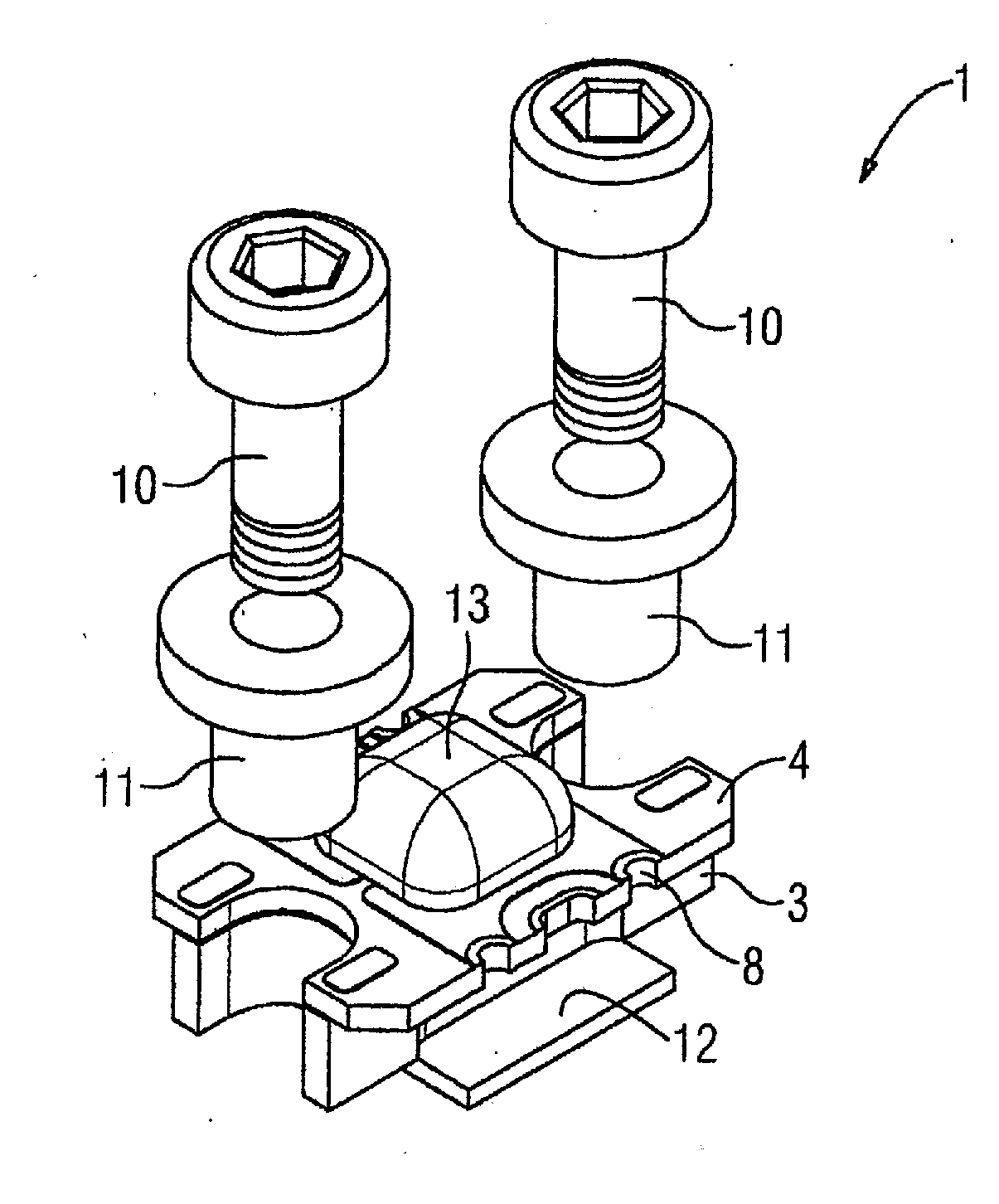
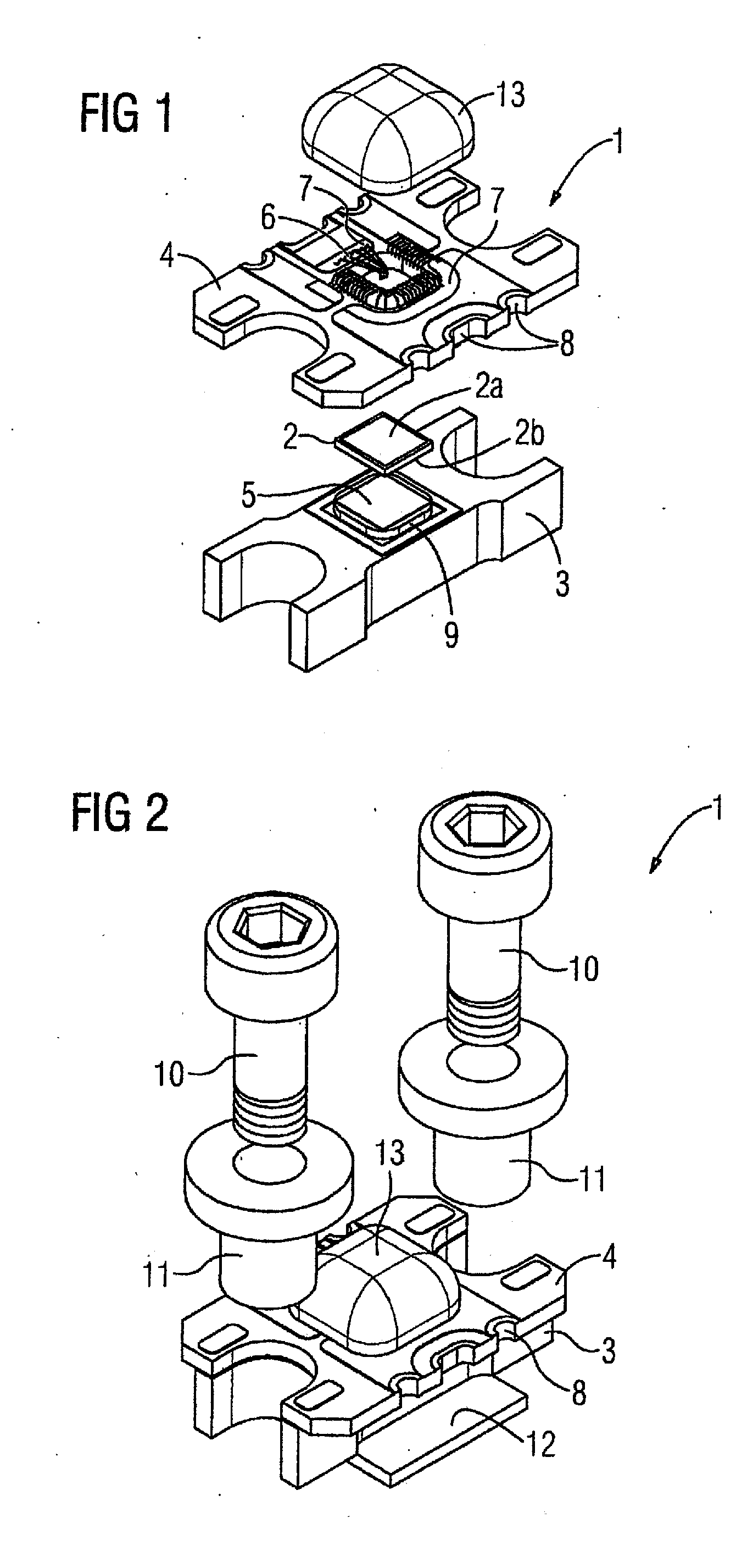
[0034]Shown in FIG. 1 is an embodiment of the chip package assembly 1 in accordance with the present invention, for mounting at least one semiconductor chip 2. The chip package assembly 1 comprises a semiconductor chip 2, particularly with transistor connections, for example, for the gate and source on the top side of the chip 2a and with drain connection on the bottom side of the chip 2b. The chip package assembly 1 further comprises a flange 3, on which the semiconductor chip 2 and a substrate 4 are arranged on one side. The flange 3 operates as a cooling device, which has a good thermal conductivity.

[0035]During usage, the semiconductor chip 2 produces waste heat. In high power applications the waste heat can increase the temperature of the semiconductor chip 2 and damage it. This is why heat must be removed and transferred to the environment, to cool down the semiconductor chip 2 and / or to keep the temperature of the semiconductor chip 2 below a critical temperature. Above the c...


PUM

PropertyMeasurementUnit
electricalaaaaaaaaaa
thermally conductingaaaaaaaaaa
conductingaaaaaaaaaa

Abstract

A chip package assembly and its use for mounting and demounting of at least one semiconductor chip that includes a flange and a substrate, where the at least one chip and the substrate are arranged on one side of the flange, and where the flange is composed of an electrical and thermally conducting material.

Description

CROSS-REFERENCE TO RELATED APPLICATIONS [0001]This is a U.S. national stage of application No. PCT / RU2013 / 000031 filed 16 Jan. 2013.BACKGROUND OF THE INVENTION [0002]1. Field of the Invention[0003]The present invention relates to chip packages and, more particularly, to a chip package assembly and its use for mounting at least one semiconductor chip, comprising a flange and a substrate, where the at least one semiconductor chip and the substrate are arranged on one side of the flange.[0004]The present invention describes a chip package assembly which can be used for mounting and encapsulation of semiconductor chips containing for example vertical junction field effect transistors (VJFET).[0005]2. Description of the Related Art[0006]Inter alia high power RF semiconductor devices can be composed of VJFET structures. Chip packages are known, for example, from U.S. Pat. No. 6,318,622B1, U.S. Pat. No. 6,967,400B2, U.S. Pat. No. 6,465,883B2 and U.S. Pat. No. 7,256,494B2.[0007]In U.S. Pat....

Claims


Application Information

Patent Timeline
Patent Type & Authority Applications(United States)
IPC IPC(8): H01L23/367H05K3/34H01L23/31H01L23/498H01L23/373
CPCH01L23/367H01L23/49838H01L23/3736Y10T29/49131H01L23/49811H05K3/34H01L23/3121H01L23/3735H01L2924/0002H01L2224/48091H01L2224/49171H01L23/047H01L2924/00014H01L2924/00
Inventor IVANOV, EVGENYKRASNOV, ANDREYSHARKOV, GEORGYTIKHOMIROVA, NADEZHDA
Owner SIEMENS RES CENT LIMITED LIABILITY
Why Eureka
Try Eureka