System and method for temperature sensing of three-dimensional integrated circuit

a technology of three-dimensional integrated circuits and temperature sensing systems, applied in the direction of instruments, heat measurement, calorimeters, etc., can solve the problems of increasing the design complexity increasing the complexity of the need for a large number of through silicon vias, so as to reduce the complexity of the semiconductor manufacturing of three-dimensional integrated circuits and the implementation cost of the temperature sensing system. , the effect o

Active Publication Date: 2015-12-24
NAT CHENG KUNG UNIV
View PDF1 Cites 8 Cited by
  • Summary
  • Abstract
  • Description
  • Claims
  • Application Information

AI Technical Summary

Benefits of technology

[0016]The system and the method for temperature sensing of three-dimensional integrated circuits of the present invention uses Through Silicon Vias (TSV) to conduct the temperature of various points at different chip layers to a master layer for measurement and calibration. The TSVs are formed by Copper Damascene utilized in a back-end of semiconductor manufacturing. Thus both the design complexity and the implementation cost of the temperature sensing system are reduced. Moreover, under the assistance of the TSVs, the temperature sensors of the system for temperature sensing of three-dimensional integrated circuits are all arranged at the master layer with the same manufacturing process while heat of each point at slave layers with different manufacturing processes is conducted to a corresponding temperature sensing circuit of the master layer through the TSVs for temperature measurement. Thereby the complexity of the semiconductor manufacturing of three-dimensional integrated circuit is reduced. Furthermore, the TSVs of the present invention are used in the way different from the conventional through silicon vias for heat dissipation. The temperature of the positions at the slave layers to be detected is conducted to the master layer. Thus there is no need to use through silicon vias with large diameter for temperature conduction. Therefore the system for temperature sensing of three-dimensional integrated circuits of the present invention will not occupy too much chip area and the chip size can be minimized significantly. At last, all temperature sensors are disposed on the master layer manufactured by the same process. Thus not only the temperature sensor architecture is convenient and easy to be selected, the multiple temperature sensing mechanism for two-dimensional SoC available now can be used smoothly in the 3D IC integrated system. At the same time, the calibration of respective temperature circuit needs no through silicon vias for signal transmission. The manufacturing cost of the chip is reduced.

Problems solved by technology

However, one of the big challenges facing 3D IC is how to remove the heat generated by various chip layers to keep a high performance chip temperature within the system and reliability constraints and prevent hot spots.
As a result, different chip layers have different temperature sensors and the design complexity of the temperature sensing system is increased dramatically.
Thus the calibration of all temperature sensors in the temperature sensing system is getting quite difficult and a lot of Through Silicon Vias may be required.
Thus for companies and researchers dedicated to 3D IC related temperature sensing technology, it is an important issue to invent a temperature sensing system for 3D ICs with low cost and low complexity in which temperature sensors are arranged at different chip layers of 3D IC.

Method used


Image

  • System and method for temperature sensing of three-dimensional integrated circuit
  • System and method for temperature sensing of three-dimensional integrated circuit
  • System and method for temperature sensing of three-dimensional integrated circuit

Examples


Embodiment Construction

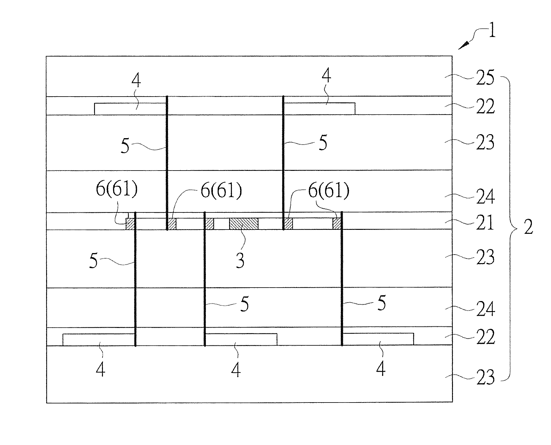
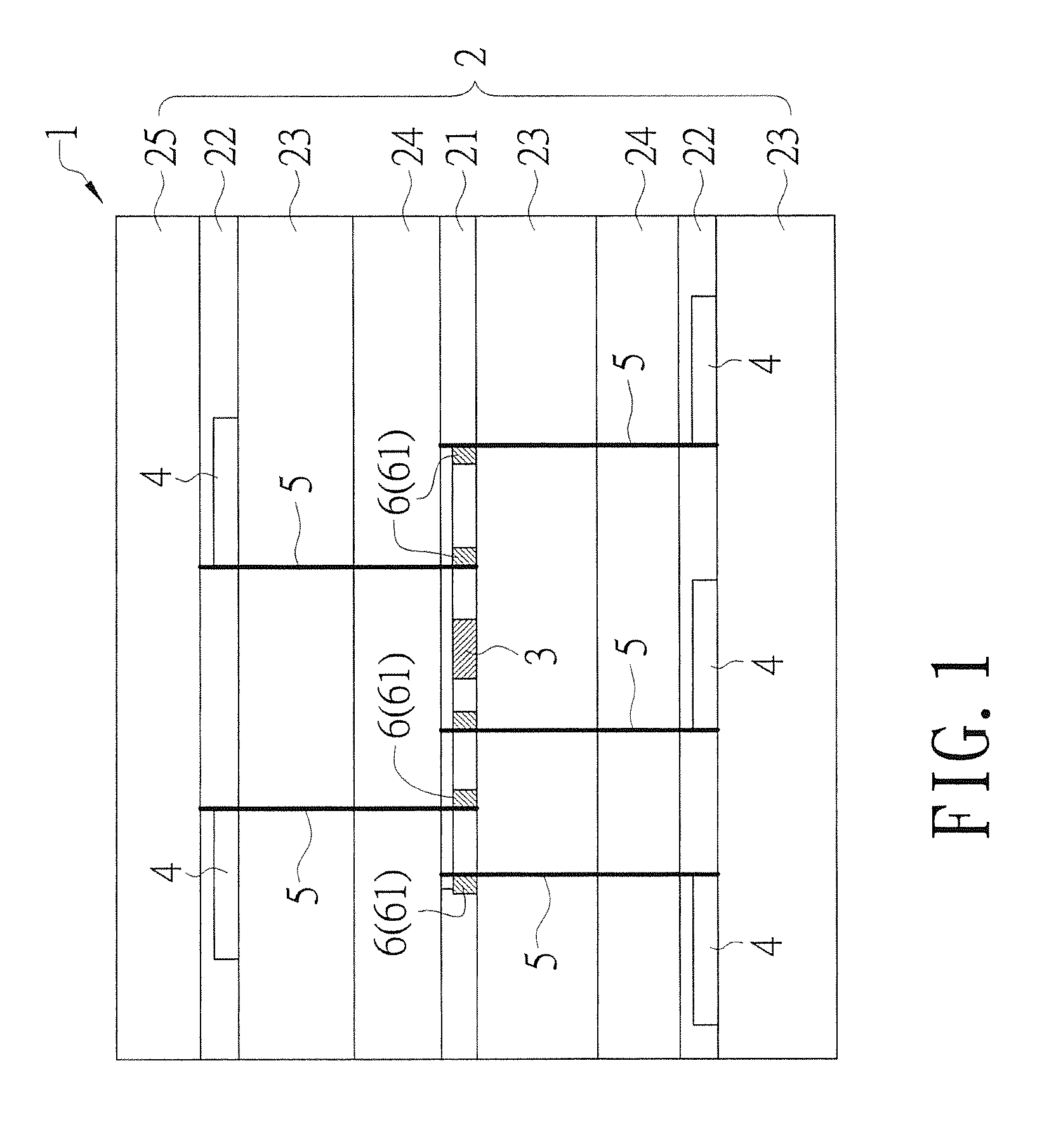
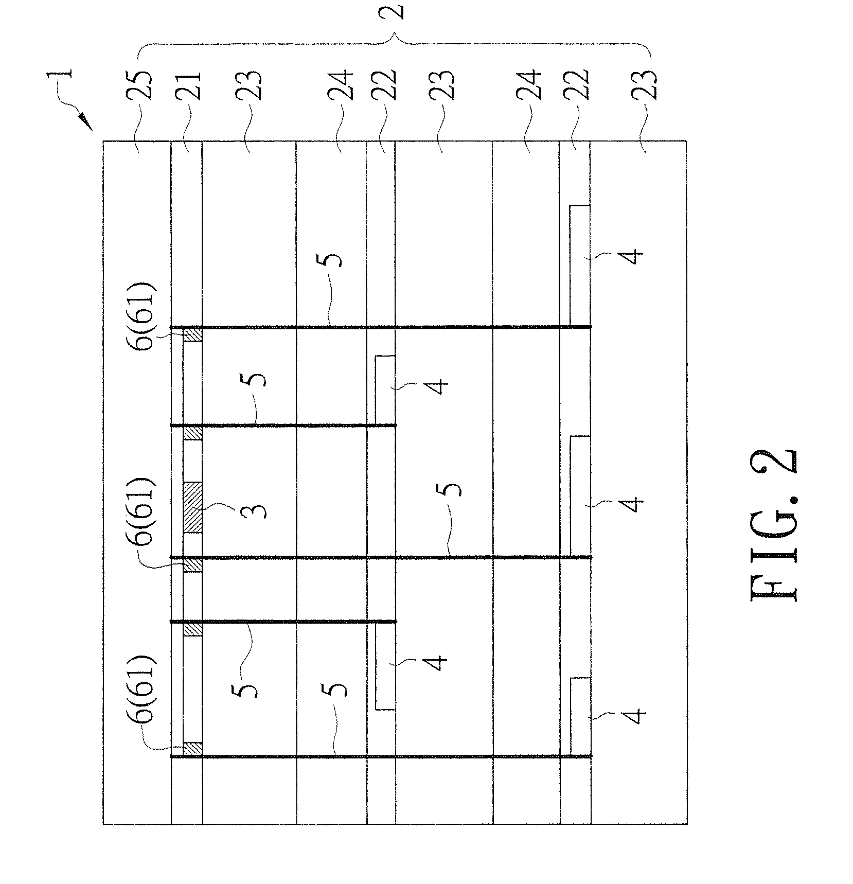
[0021]Refer to FIG. 1, a schematic drawing showing structure of a system for temperature sensing of three-dimensional integrated circuits according to the present invention is revealed. A three-dimensional integrated circuits (3D IC) 1 is formed by stacking of a plurality of chip layers 2 each of which executes specific function. The chip layer 2 includes a master layer 21 and at least one slave layer 22. A master temperature sensor 3 is disposed on the master layer 21 and a first thermal conductive part 4 is set on the slave layer 22 and located at the position where heat is detected. The master temperature sensor 3 and the first thermal conductive part 4 are connected to each other by a thermal conductive structure 5. In an embodiment of the present invention, the master layer 21 and the slave layer 22 are formed on a substrate 23 respectively while a dielectric layer 24 is stacked between the master layer 21 and the slave layer 22. A protective layer 25 is formed on the outermost...


PUM

PropertyMeasurementUnit
thermal conductiveaaaaaaaaaa
temperatureaaaaaaaaaa
diameteraaaaaaaaaa

Abstract

A system and a method for temperature sensing of three-dimensional integrated circuits are revealed. The three-dimensional integrated circuit is formed by stacking of a plurality of chip layers that execute specific functions. The chip layer includes a master layer and at least one slave layer. The master layer is disposed with a master temperature sensor while a first thermal conductive part is arranged at the slave layer where heat is detected. The first thermal conductive part and the master temperature sensor are connected by a thermal conductive structure. Thereby temperature of various points at different chip layers is conducted to the same chip layer by Through Silicon Vias to be measured and calibrated. The design complexity and the implementation cost of the temperature sensing system are significantly reduced.

Description

BACKGROUND OF THE INVENTION[0001]1. Fields of the Invention[0002]The present invention relates to a system and a method for temperature sensing of three-dimensional integrated circuits, especially to a system and a method for multiple temperature sensing of a plurality of chip layers of three-dimensional integrated circuits. In the system, temperature of various points at different chip layers is conducted to the same chip layer by Through Silicon Vias (TSVs) to be measured and calibrated. The design complexity and the implementation cost of the temperature sensing system can be reduced significantly.[0003]20 Descriptions of Related Art[0004]The three-dimensional integrated circuit (3D IC) can solve the problems of two-dimensional system-on-chip (SoC) by Through Silicon Vias (TSVs). However, one of the big challenges facing 3D IC is how to remove the heat generated by various chip layers to keep a high performance chip temperature within the system and reliability constraints and pr...

Claims


Application Information

Patent Timeline
Patent Type & Authority Applications(United States)
IPC IPC(8): G01N25/18G01K15/00
CPCG01K15/005G01N25/18G01K1/16
Inventor CHANG, SOON-JYHCHEN, PENG-YULEE, KUEN-JONGCHEN, CHUNG-HO
Owner NAT CHENG KUNG UNIV
Why Eureka
Try Eureka