Backlight assembly and display device having the same
- Summary
- Abstract
- Description
- Claims
- Application Information
AI Technical Summary
Benefits of technology
Problems solved by technology
Method used
Image

Examples
first embodiment
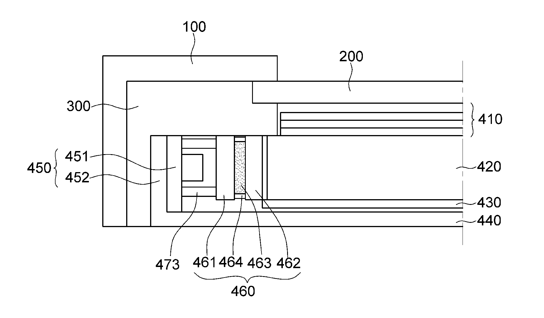
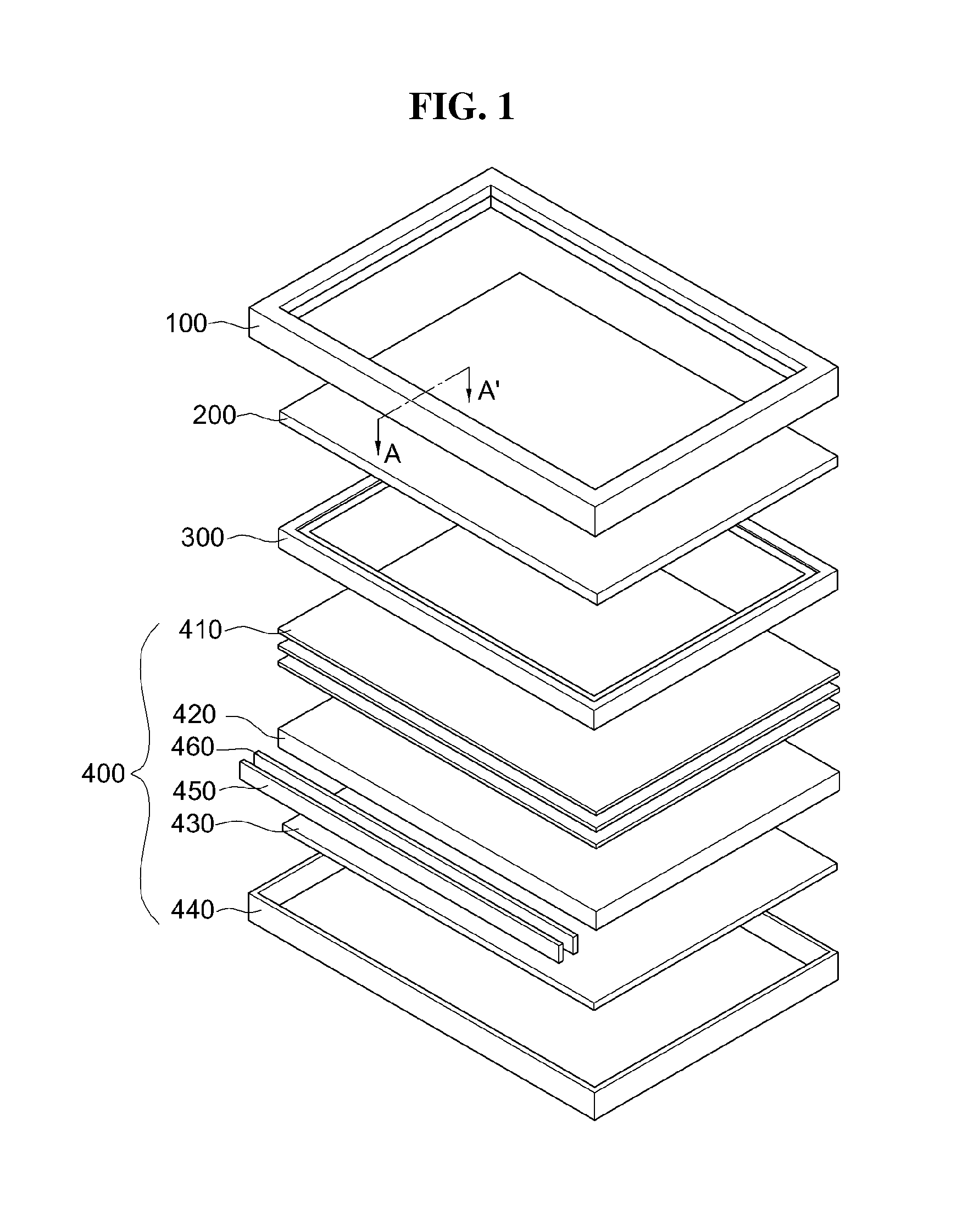
[0030]Turning now to FIGS. 1 and 2, FIG. 1 is an exploded perspective view illustrating a display device according to the present invention and FIG. 2 is a cross-sectional view taken along a line A-A′ of FIG. 1.
[0031]Referring now to FIGS. 1 and 2, the display device includes a liquid crystal panel 200 configured to display an image, a backlight assembly 400 configured to supply light to the liquid crystal panel 200, a top case 100 provided to cover the liquid crystal panel 200, and a mold frame 300 configured to connect the top case 100 to a bottom case 440 and accommodate the liquid crystal panel 200 seated thereon.
[0032]The mold frame 300 is coupled to the bottom case 440 and accommodates the liquid crystal panel 200. The mold frame 300 may be made out of a flexible material, such as plastic, in order to prevent damage to the liquid crystal panel 200.
[0033]The top case 100 is coupled to the mold frame 300 and to the bottom case 440 to cover the liquid crystal panel 200 seated on ...
second embodiment
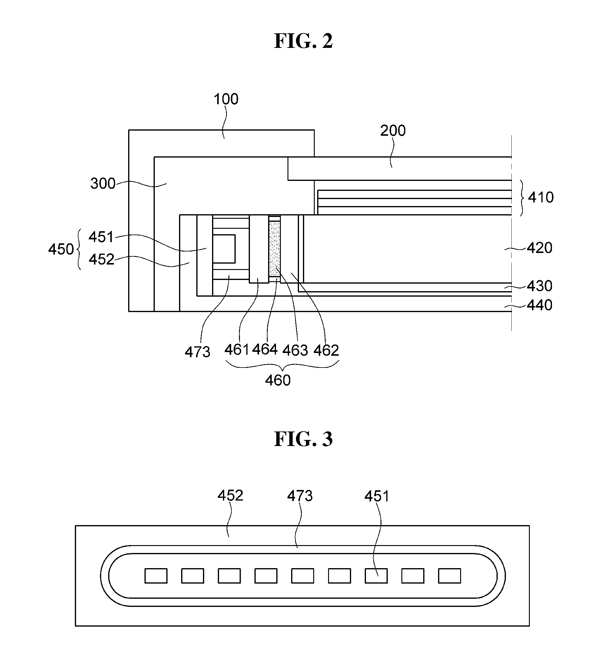
[0062]Referring now to FIG. 6, a spacer 476 according to the present invention includes a first spacer and a second spacer that face each other with a light source 451 interposed therebetween, the first and second spacers corresponding to the long side portions of the circuit substrate 452. At the short side portion of the circuit substrate 452 and unlike the spacer of FIG. 3, the spacer 476 of FIG. 6 is open.
third embodiment
[0063]Referring now to FIG. 7, a spacer 477 according to the present invention includes only portions that correspond to the short sides of the circuit substrate 452, while portions that correspond to the long sides are open. The spacers 476 and 477 of
[0064]FIGS. 6 and 7 have structures that allow a wavelength converting unit 460 to be fixed to the light source unit 450 using minimal amounts of materials.
[0065]Referring now to FIGS. 8 and 9, a metal pattern 480 is formed in addition to the spacer 478 in order to fix the wavelength converting unit 460 to the light source unit 450. In FIGS. 8 and 9, the metal patterns 480 are external to spacer 478 and are arranged closer to the short sides of circuit substrate 452 than spacer 478. The metal pattern 480 may be separately formed in order to support, along with the spacer 478, the wavelength converting unit 460. Further, instead of separately forming the metal pattern 480, a Zener diode can instead be formed on the circuit substrate 452...
PUM
 Abstract
Description
Claims
Application Information
 - Generate Ideas
- Intellectual Property
- Life Sciences
- Materials
- Tech Scout
- Unparalleled Data Quality
- Higher Quality Content
- 60% Fewer Hallucinations
Browse by: Latest US Patents, China's latest patents, Technical Efficacy Thesaurus, Application Domain, Technology Topic, Popular Technical Reports.
© 2025 PatSnap. All rights reserved.Legal|Privacy policy|Modern Slavery Act Transparency Statement|Sitemap|About US| Contact US: help@patsnap.com