Systems and methods for chip to chip communication

a chip and chip technology, applied in the field of integrated circuits, can solve the problems of protocol over-engineering, excessive use of ic area and extra power consumption, and protocol may not react quickly to changing realities, so as to reduce the aggression of variable electromagnetic interference (emi) and the effect of relatively quick change frequency

Active Publication Date: 2016-01-21
QUALCOMM INC
View PDF7 Cites 12 Cited by
  • Summary
  • Abstract
  • Description
  • Claims
  • Application Information

AI Technical Summary

Benefits of technology

[0008]Aspects disclosed in the detailed description include systems and methods for chip to chip communication. In an exemplary aspect, a chip to chip link comprises a master device having a data transmitter, a clock, a clock transmitter, a phase locked loop (PLL) associated with the clock, and a receiver. The chip to chip link also comprises a slave device that has a data transmitter, a clock receiver, and a data receiver. Noticeably absent from the slave device is a clock or a PLL. By removing the clock from the slave device, th...

Problems solved by technology

The downside of having a common protocol is that the protocol is frequently over-engineered to address “worst-case” scenarios.
Such over-engineering results in excessive use of area within an IC and extra power consumption.
An additional downside is that the protocol may not react quickly to changing realities.
That is, new technologies or unexpected combinations of old technology may interact with the protocol poorly.
An example of such poor interaction is that as clock speeds on the chip to chi...

Method used


Image

  • Systems and methods for chip to chip communication
  • Systems and methods for chip to chip communication
  • Systems and methods for chip to chip communication

Examples


Embodiment Construction

[0022]With reference now to the drawing figures, several exemplary aspects of the present disclosure are described. The word “exemplary” is used herein to mean “serving as an example, instance, or illustration.” Any aspect described herein as “exemplary” is not necessarily to be construed as preferred or advantageous over other aspects.

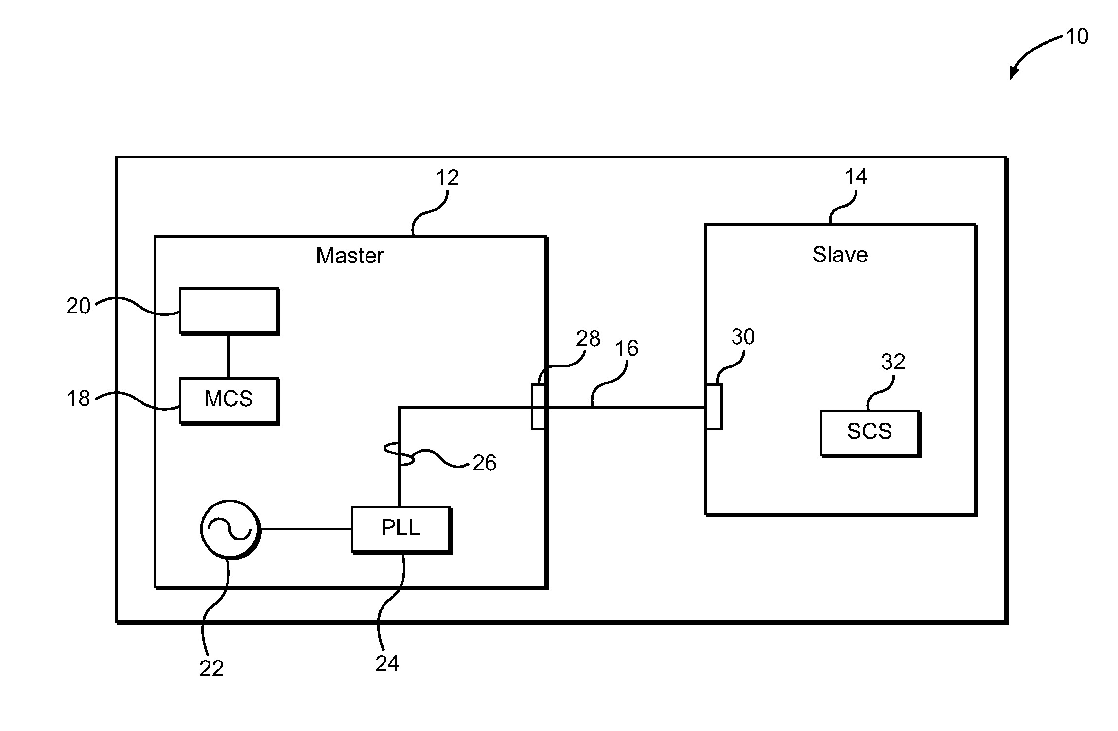
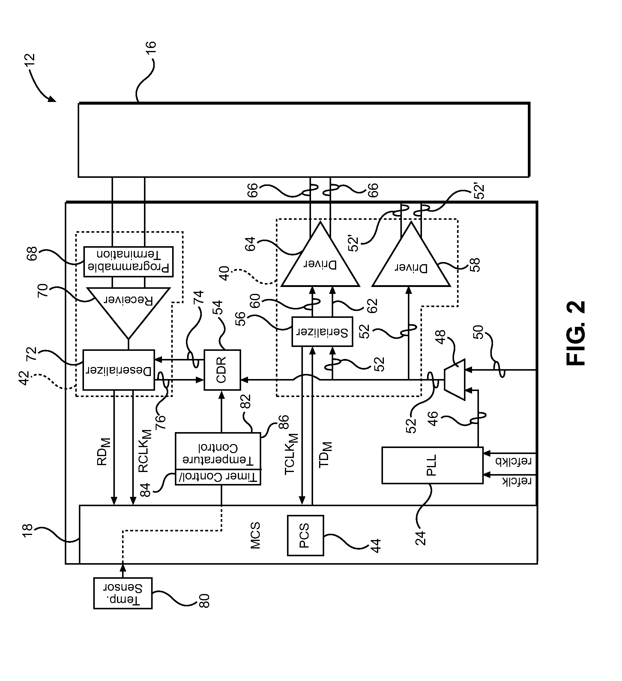
[0023]Aspects disclosed in the detailed description include systems and methods for chip to chip communication. In an exemplary aspect, a chip to chip link comprises a master device having a data transmitter, a clock, a clock transmitter, a phase locked loop (PLL) associated with the clock, and a receiver. The chip to chip link also comprises a slave device that has a data transmitter, a clock receiver, and a data receiver. Noticeably absent from the slave device is a clock or a PLL. By removing the clock from the slave device, the slave device does not have the power consuming element of a slave PLL. Further, because the slave device does not have a ...


PUM


Abstract

Systems and methods for chip to chip communication are disclosed. In an exemplary aspect, a chip to chip link comprises a master device having a data transmitter, a clock, a clock transmitter, a phase locked loop (PLL) associated with the clock, and a receiver. The chip to chip link also comprises a slave device that has a data transmitter, a clock receiver, and a data receiver. Noticeably absent from the slave device is a clock or a PLL. By removing the clock from the slave device, the slave device does not have the power consuming element of a slave PLL. Further, because the slave device does not have a clock which would normally have to acquire a new frequency and settle, the master clock may change frequency relatively quickly and vary the frequency across many frequencies, not just one or two predefined frequencies.

Description

PRIORITY CLAIM[0001]The present application claims priority to U.S. Provisional Patent Application Ser. No. 62 / 026,063 filed on Jul. 18, 2014 and entitled “SYSTEMS AND METHODS FOR CHIP TO CHIP COMMUNICATION,” which is incorporated herein by reference in its entirety.BACKGROUND[0002]I. Field of the Disclosure[0003]The technology of the disclosure relates generally to integrated circuits (ICs) and particularly to communication between two ICs.[0004]II. Background[0005]Computing devices are prevalent in contemporary society. Such computing devices benefit from an increasing array of functionality being made available by virtue of increasingly complex integrated circuits (ICs). Such ICs may be positioned on a printed circuit board (PCB) and interconnected through non-transitory conductive elements, for example, physical traces. Signals are routed onto these physical traces according to predefined protocols. The increased functionality increases the amount of data that is included in suc...

Claims


Application Information

Patent Timeline
IPC IPC(8): G06F1/08G06F13/42G06F13/364
CPCG06F13/4291G06F13/364G06F1/08Y02D10/00
Inventor THURSTON, JASON ALANARCUDIA, KENNETH LUIS
Owner QUALCOMM INC
Why Eureka
Try Eureka