Voltage controlled oscillator

a voltage control and oscillator technology, applied in the direction of oscillator, electrical equipment, etc., can solve the problems of inability to control the frequency around the desired gate voltage, the inability to set the capacitance switching voltage as desired, etc., and achieve the effect of simplifying the design

Inactive Publication Date: 2006-01-26
PANASONIC CORP
View PDF8 Cites 16 Cited by
  • Summary
  • Abstract
  • Description
  • Claims
  • Application Information

AI Technical Summary

Benefits of technology

[0052] A voltage controlled oscillator according to the present invention can thus control the capacitance switching voltage independently of the temperature compensation control signal and the external voltage frequency control signal, and can thus vary the frequency around a desired control voltage.
[0053] The present invention further advantageously enables inputting a signal for cancelling threshold voltage variation and the temperature characteristic of the MOS transistor independently of the temperature compensation control signal and the external voltage frequency control signal, simplifying the design of a temperature compensation control circuit and an external voltage frequency control circuit, and achieving a voltage controlled oscillator that uses the electrostatic capacitance produced between the source / drain and gate terminals of a MOS transistor of which the source and drain are shorted.

Problems solved by technology

A first problem with the foregoing art is that because the dc bias of the source / drain terminal is determined on the amplifier side of the oscillator circuit, the capacitance switching voltage cannot be set as desired and the frequency cannot be controlled around a desired gate voltage.
A second problem is that the capacitance switching voltage is dependent upon the temperature characteristic and variation in the threshold voltage of a MOS transistor manufactured in a conventional CMOS process, but the temperature compensation control signal and the external voltage frequency control signal in the prior art must be able to cancel the temperature characteristic and threshold voltage variation of the MOS transistor.

Method used


Image

  • Voltage controlled oscillator
  • Voltage controlled oscillator
  • Voltage controlled oscillator

Examples


embodiment 1

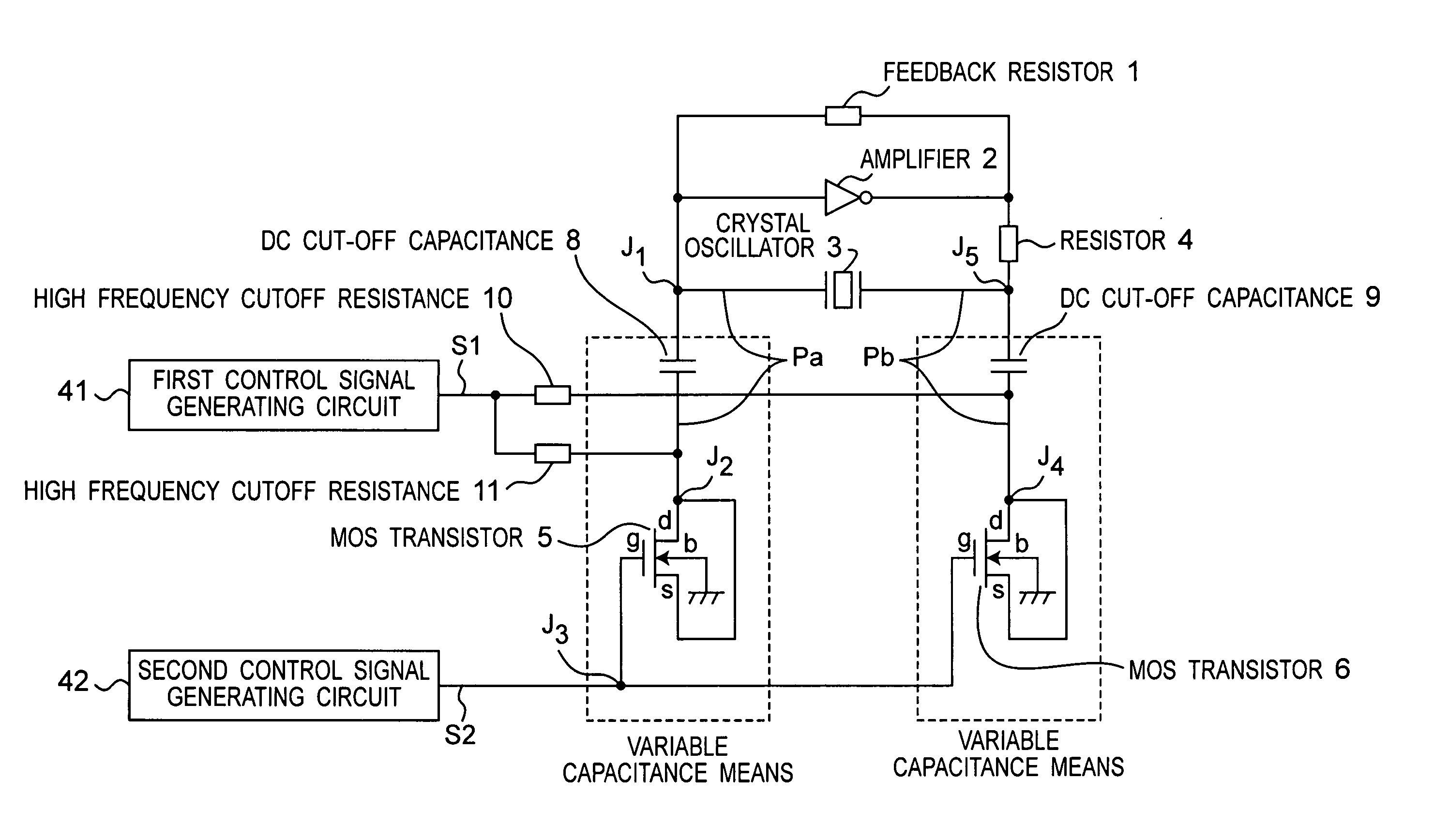
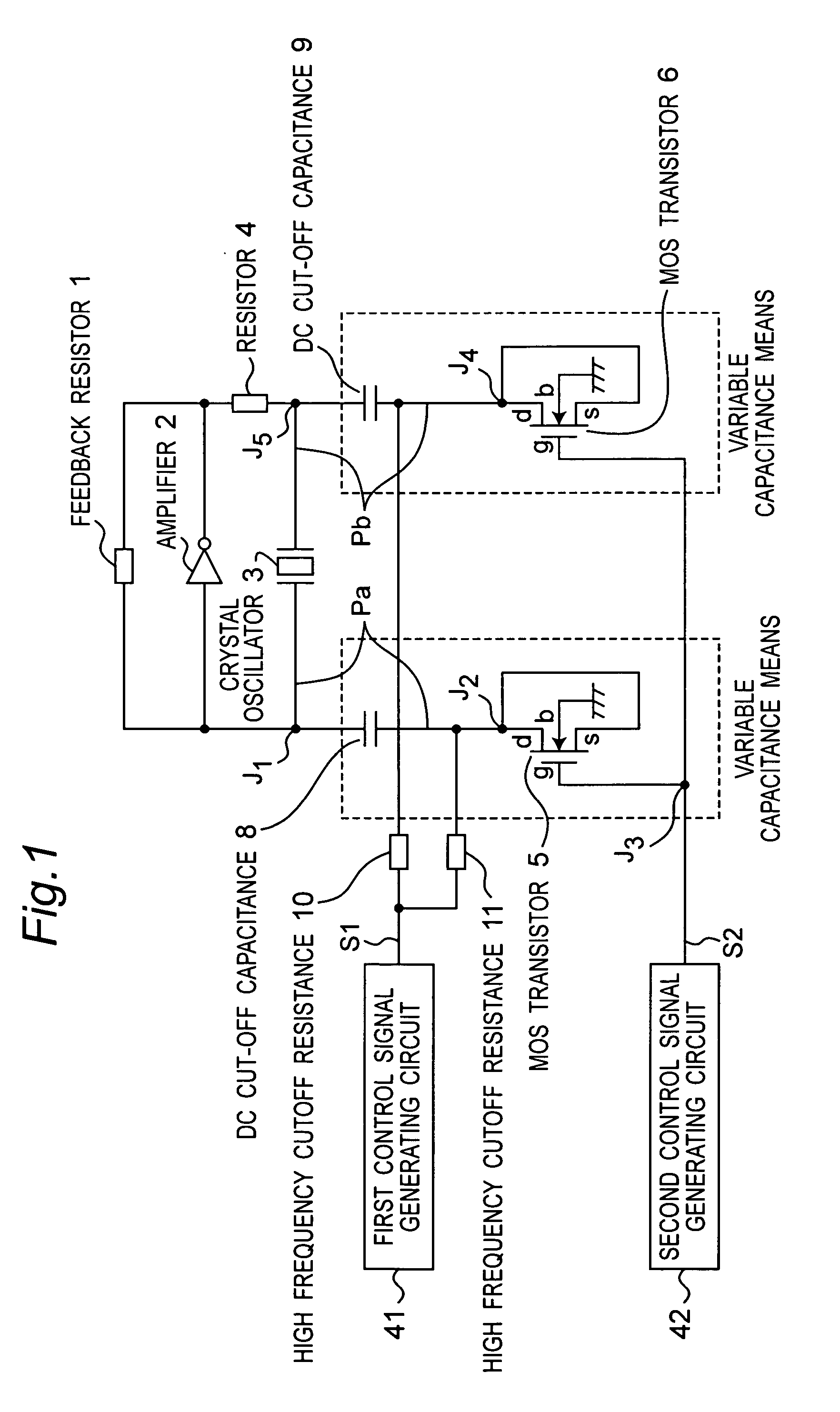
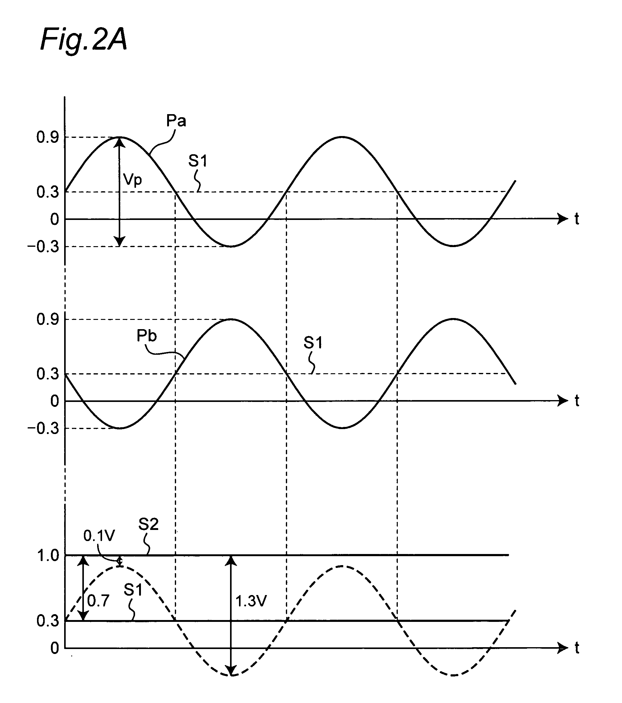
[0070]FIG. 1 is a circuit diagram showing the arrangement of a voltage controlled oscillator according to a first embodiment of the present invention. MOS transistors 5 and 6 are used as a variable capacitance in this first embodiment of the invention. Using MOS transistor 5 by way of example, the source s and drain d are shorted and the back gate b goes to ground. As described below, the capacitance between the source / drain and gate is variable. MOS transistor 5 is thus used as a variable capacitance device in the present invention. MOS transistor 6 is identical to MOS transistor 5.

[0071] As shown in FIG. 1, the oscillator circuit is composed of a feedback resistor 1 constituting a feedback circuit, an amplifier 2, and a crystal oscillator 3. The load capacitance of the oscillator circuit is the capacitance of the oscillation loop, which is the closed loop from one terminal of the crystal oscillator 3 to node J1, DC cut-off capacitance 8, node J2, MOS transistor 5, node J3, MOS tr...

embodiment 2

[0097]FIG. 5A is a schematic circuit diagram showing a voltage controlled oscillator according to a second embodiment of the present invention. As shown in FIG. 5A, the load capacitance of this oscillator circuit is the variable capacitance means composed of the first DC cut-off capacitance 8, variable capacitance MOS transistor 13, and a second DC cut-off capacitance 9 serial connected between the terminals of the crystal oscillator 3. The variable capacitance of this oscillator is the electrostatic capacitance produced between the source / drain and gate terminals of a MOS transistor 13 of which the source and drain are shorted. An arrangement in which an opposite phase oscillation voltage is applied to the source / drain and gate terminals is also possible.

[0098] A fourth control signal generating circuit 44 applies a fourth control signal S4 through high frequency cutoff resistance 14 to the source / drain terminal of MOS transistor 13. A fifth control signal generating circuit 45 ap...

embodiment 3

[0108]FIG. 9 is a schematic circuit diagram of a voltage controlled oscillator according to a third embodiment of the present invention. As shown in FIG. 9, this embodiment differs from the arrangement shown in FIG. 1 in that a variation cancellation circuit 20 is additionally disposed between the first control signal generating circuit 41 and high frequency cutoff resistance 10.

[0109] This variation cancellation circuit 20 is composed of MOS transistor 25, resistances 21, 22,26, 28, transistors 23, 24, and inversion amplifier 27. MOS transistor 25 is rendered near MOS transistors 5 and 6 and has the same IC structure and characteristics as MOS transistors 5 and 6. Voltage change due to temperature or variations in the MOS transistor 25 is inverted by the inversion amplifier 27 to a negative change. Voltage change due to temperature or variations in MOS transistors 5 and 6 appears as a positive at the drain and source of MOS transistors 5 and 6. These positive and negative changes ...


PUM


Abstract

A voltage controlled oscillator enables controlling the MOS transistor threshold voltage independently of the temperature compensation control signal and external voltage frequency control signal. The voltage controlled oscillator has a crystal oscillator and a load capacitance is parallel connected to a crystal oscillator. The load capacitance includes a first MOS transistor comprising a gate terminal and a source/drain terminal formed by shorting the source and drain, and a second MOS transistor comprising a gate terminal and a source/drain terminal formed by shorting the source and drain. First and second control signal generating circuits supply respective control signals to the source/drain terminals and gate terminals of the first and second MOS transistors.

Description

BACKGROUND OF THE INVENTION [0001] 1. Field of Technology [0002] The present invention relates to a voltage controlled oscillator which is used as a voltage controlled temperature compensated crystal oscillator. [0003] 2. Description of Related Art [0004] A temperature compensated crystal oscillators is a type of crystal oscillator that is used as a reference frequency source in cell phones and other electronic devices, and reduces change in output frequency resulting from temperature variations. A voltage controlled oscillator is a type of oscillator that can change the load capacity and control the output frequency by providing a variable capacitor, which can change the capacitance by means of voltage, as a load capacitance in the oscillation loop and controlling the terminal voltage of this variable capacitance. A temperature compensated crystal oscillator controls the terminal voltage of the variable capacitance in a voltage controlled oscillator to cancel the temperature charac...

Claims


Application Information

Patent Timeline
Patent Type & Authority Applications(United States)
IPC IPC(8): H03B5/32
CPCH03B5/04H03B2200/0012H03B5/366
Inventor OOTSUKA, TAKASHITAKEUCHI, HISATOSHINGU, KEIGO
Owner PANASONIC CORP
Why Eureka
Try Eureka