Receiver Circuitry and Method for Converting an Input Signal From a Source Voltage Domain Into an Output Signal for a Destination Voltage Domain

a receiver circuit and input signal technology, applied in logic circuits using dielectric elements, electrical apparatus, coupling/interface using field-effect transistors, etc., can solve the problem of still a possibility of certain components suffering from overstress in particular situations, and achieve the effect of reducing the margin between vih and vil levels, increasing the margin, and being more robust against such nois

Active Publication Date: 2016-02-04
ARM LTD
View PDF4 Cites 14 Cited by
  • Summary
  • Abstract
  • Description
  • Claims
  • Application Information

AI Technical Summary

Benefits of technology

[0023]In some implementations, it may be the case that noise and the like serve to reduce the margin between the VIH and VIL levels. In such embodiments, the signal evaluation circuitry may further comprise hysteresis generation circuitry configured to provide an increased margin between the logic high voltage threshold and the logic low voltage threshold established by the signal evaluation circuitry, thereby making the syste...

Problems solved by technology

Whilst the operation of the first and second internal signal generation circuits ensures that the generated first and second internal signals provided as inputs to the signal evaluation circuitry will not exceed the stressing threshold of the components wi...

Method used


Image

  • Receiver Circuitry and Method for Converting an Input Signal From a Source Voltage Domain Into an Output Signal for a Destination Voltage Domain
  • Receiver Circuitry and Method for Converting an Input Signal From a Source Voltage Domain Into an Output Signal for a Destination Voltage Domain
  • Receiver Circuitry and Method for Converting an Input Signal From a Source Voltage Domain Into an Output Signal for a Destination Voltage Domain

Examples


Embodiment Construction

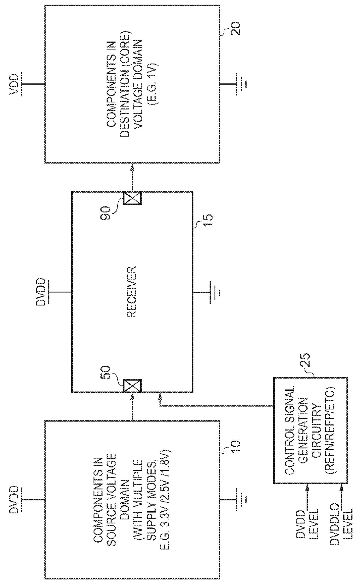
[0039]FIG. 1 is a block diagram of a system incorporating a receiver in accordance with one embodiment. As shown, a source voltage domain 10 will include a number of components operating from a supply voltage of the source voltage domain, also referred to herein as DVDD. The reference voltage provided to the source voltage domain is a ground connection, and accordingly signals generated by components in the source voltage domain may vary in a voltage range between DVDD and 0V.

[0040]In accordance with the embodiment shown in FIG. 1, a signal generated in the source voltage domain needs to be propagated to one or more components in a destination voltage domain 20, also referred to herein as a core voltage domain. The core voltage domain operates from a supply voltage VDD, and also receives as its reference voltage a ground connection, so that signals in the destination voltage domain vary in the range between VDD and 0V.

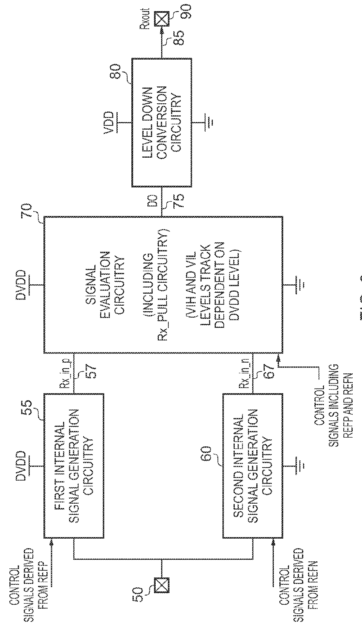
[0041]The receiver circuitry receives at an input connection 50 (...


PUM


Abstract

The present invention provides a receiver circuit and method for receiving an input signal from a source voltage domain and converting the input signal into an output signal for a destination voltage domain. The source voltage domain operates from a supply voltage that exceeds a stressing threshold of components within the receiver circuitry, and the receiver circuitry is configured to operate from the supply voltage of the source voltage domain. The receiver circuitry comprises first internal signal generation circuitry configured to convert the input signal into a first internal signal in a first voltage range, and second internal signal generation circuitry configured to convert the input signal into a second internal signal in a second voltage range. Signal evaluation circuitry establishes a logic high voltage threshold and a logic low voltage threshold dependent on the supply voltage, and employs the first and second internal signals in order to detect based on the logic high voltage threshold and logic low voltage threshold when the input signal transitions between a logic low level and a logic high level (in either direction). Output generation circuitry then generates the output signal in dependence on the detection performed by the signal evaluation circuitry. The first voltage range and the second voltage range are such that the first internal signal and second internal signal will not exceed the stressing threshold of components in the signal evaluation circuitry. The receiver circuitry is able to reliably detect transitions in the input signal in situations where the supply voltage of the source voltage domain exceeds the stressing threshold of the receiver's components, but without overstress of the receiver's components.

Description

FIELD OF THE INVENTION[0001]The present invention relates to a receiver circuit and method for converting an input signal from a source voltage domain into an output signal for a destination voltage domain, in particular in situations where the source voltage domain uses a higher supply voltage than the destination voltage domain.BACKGROUND OF THE INVENTION[0002]In traditional designs of receiver circuitry, the receiver circuitry is configured to operate from a supply voltage that matches the “native voltage” (also referred to as a “technology limit value”) of the components within the receiver circuitry. The voltage drop across any terminals of the components that make up the receiver circuitry should be lower than the native voltage in order to prevent damage due to overstress, which may in turn lead to reduced reliability. For example, if the receiver circuitry is constructed from CMOS devices with a native voltage of 1.8V, the receiver circuitry will typically utilise a 1.8V sup...

Claims


Application Information

Patent Timeline
IPC IPC(8): H03K19/0185
CPCH03K19/018521H03K19/00315
Inventor DEY, RANABIRVINUKONDA, VIJAYA KUMARRIEN, MIKAEL
Owner ARM LTD
Why Eureka
Try Eureka