Touch display device, driving method thereof and manufacturing method thereof

a technology of touch display and driving method, which is applied in the direction of electric digital data processing, instruments, computing, etc., can solve the problems of affecting the value of received touch sensing signals, and adding to the load of user portability, so as to reduce the thickness and weight of the display panel

Inactive Publication Date: 2016-03-03
ILI TECHNOLOGY CORPORATION
View PDF20 Cites 10 Cited by
  • Summary
  • Abstract
  • Description
  • Claims
  • Application Information

AI Technical Summary

Benefits of technology

[0006]The primary object of the present invention is to provide a touch display device that simultaneously reduces the thickness and the weight of a display panel integrated with a touch function without degrading functions of the display panel.
[0010]In the touch display device of the present invention, the metal lines may be utilized to transmit touch display signals including touch driving signal and pixel voltage signals or pixel switch signals. Therefore, in addition to serving as conducting lines that the display panel uses for transmitting pixel voltage signals or pixel switch signals, the metal lines can also form touch sensing devices with the second electrode strips. As such, a touch electrode layer for transmitting touch signals can be omitted in the touch display device of the present invention, thereby effectively reducing the thickness and the manufacturing costs of the touch display device. Further, in the present invention, with the first electrode strips disposed between the metal lines and the second electrode strips, coupling capacitance between the metal lines and the second electrode strips can be increased, and the touch sensitivity of the touch sensing devices can also be enhanced.

Problems solved by technology

Thus, the overall thickness and the weight of the panel are greater than those of one single display panel, adding to a load in user portability.
Therefore, not only the value of received touch sensing signals is affected but also the sensitivity of touch sensing devices is limited.

Method used


Image

  • Touch display device, driving method thereof and manufacturing method thereof
  • Touch display device, driving method thereof and manufacturing method thereof
  • Touch display device, driving method thereof and manufacturing method thereof

Examples


Embodiment Construction

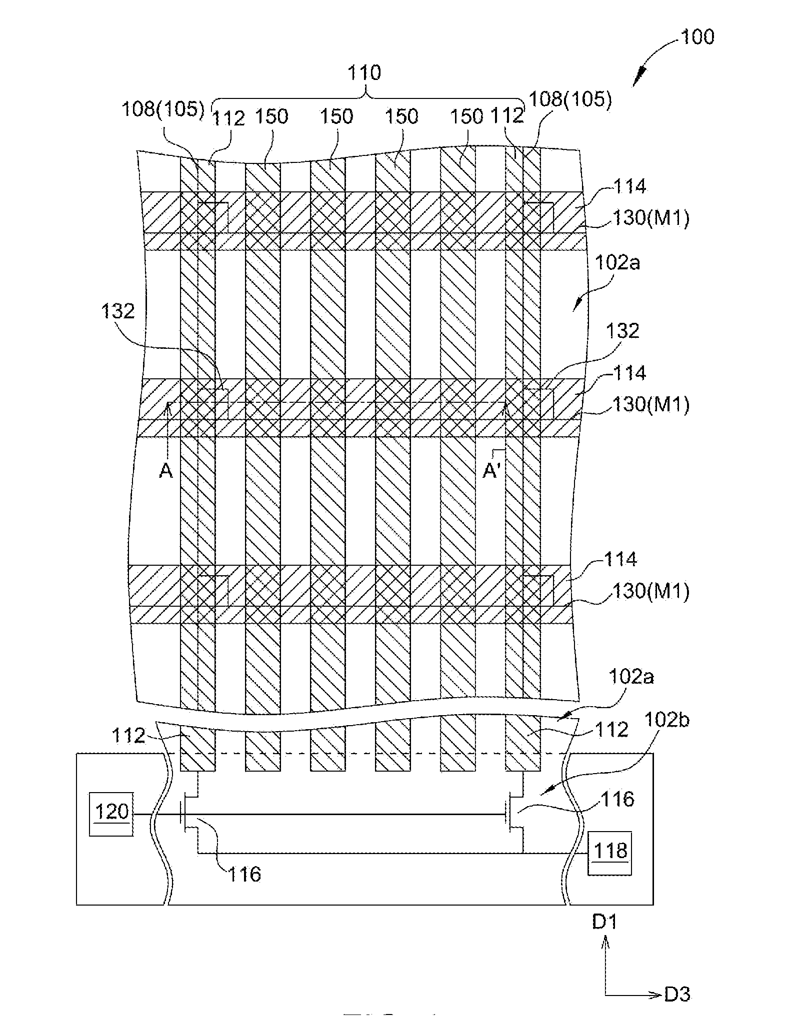
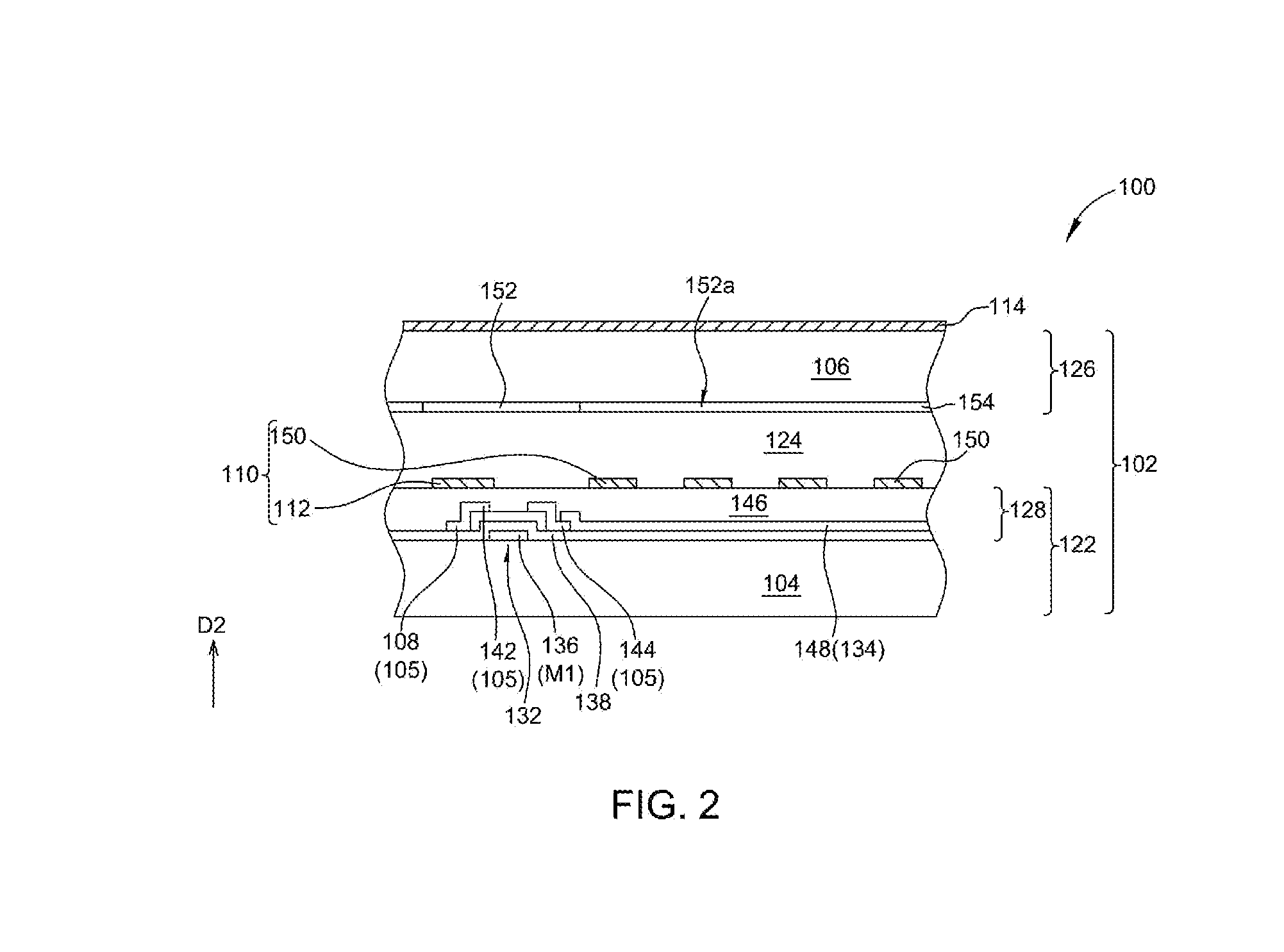
[0027]Referring to FIG. 1 and FIG. 2, according to a first embodiment of the present invention, a touch display device 100 includes a display panel 102. The display panel 102 has an active region 102a and a border region 102b, and includes a first substrate 104, a conductive layer 105 and a first transparent layer 110. The conductive layer 105 is disposed on the first substrate 104, and includes a plurality of metal lines 108. The metal lines 108 are disposed in the active region 102a, extend along a first direction D1, and are insulated from one another. The first transparent layer 110 is disposed on the conductive layer 105, and includes a plurality of first electrode strips 112. The first electrode strips 112 are disposed in the active region 102a, extend along the first direction D1, and individually overlap with at least one of the metal lines 108 in a second direction D2 substantially perpendicular to the first substrate 104, such that the first electrode strips 112 couple wit...


PUM


Abstract

A touch display device includes a substrate, a conductive layer and a transparent layer. The conductive layer is disposed on the substrate layer, and includes a plurality of metal lines, which extend along a first direction and are insulated from one another. The transparent layer is disposed on the conductive layer, and includes a plurality of first electrode strips, which extend along the first direction and individually overlap with at least one of the metal lines in a second direction substantially perpendicular to the substrate. The first electrode strips are disposed between a plurality of second electrode strips and the metal lines. The second electrode strips extend along a third direction different from the first direction and are disposed above the transparent layer. The second electrode strips form capacitance coupling with the metal lines via the first electrode strips to perform touch sensing.

Description

[0001]This application claims the benefit of U.S. Provisional Application Ser. No. 62 / 043,430, filed Aug. 29, 2014, and Taiwan Application Serial No. 103142447, filed Dec. 5, 2014, the subject matter of which is incorporated herein by reference.BACKGROUND OF THE INVENTION[0002]1. Field of the Invention[0003]The invention relates in general to a touch display device, a driving method thereof and a manufacturing method thereof, and more particularly, to a touch display device that utilizes a conductive layer of a display panel and a transparent layer on the display panel as touch sensing devices, a driving method and a manufacturing method thereof.[0004]2. Description of the Related Art[0005]A conventional touch display device is formed by directly adhering a touch panel to a display panel by an optical adhesive. Thus, the overall thickness and the weight of the panel are greater than those of one single display panel, adding to a load in user portability. In a current touch panel int...

Claims


Application Information

Patent Timeline
Patent Type & Authority Applications(United States)
IPC IPC(8): G06F3/044
CPCG06F2203/04103G06F3/044G06F3/0412G06F3/0445G06F3/0446
Inventor LIU, CHI, KANGCHAN, PING-YUHONG, GUO-KIANG
Owner ILI TECHNOLOGY CORPORATION
Why Eureka
Try Eureka