Metallic gratings and measurement methods thereof

a technology of metal gratings and gratings, applied in the field of gratings and measurement methods, can solve the problems of increasing overall costs and yield loss, and achieve the effects of increasing overall costs, reducing critical dimensions of device structures, and increasing semiconductor device density

Active Publication Date: 2016-03-10
THE RES FOUND OF STATE UNIV OF NEW YORK
View PDF63 Cites 5 Cited by
  • Summary
  • Abstract
  • Description
  • Claims
  • Application Information

AI Technical Summary

Benefits of technology

[0003]Over the past several decades, the semiconductor industry has continued to increase semiconductor device density by reducing critical dimensions of device structures, such as transistors. During the fabrication of semiconductor devices, structures mu

Problems solved by technology

Deviation from the specified tolerances will lead to f

Method used


Image

  • Metallic gratings and measurement methods thereof
  • Metallic gratings and measurement methods thereof
  • Metallic gratings and measurement methods thereof

Examples


Embodiment Construction

[0024]Aspects of the present disclosure and certain features, advantages, and details thereof, are explained more fully below with reference to the non-limiting examples illustrated in the accompanying drawings. Descriptions of well-known materials, fabrication tools, processing techniques, etc., are omitted so as not to unnecessarily obscure the disclosure in detail. It should be understood, however, that the detailed description and the specific examples, while indicating aspects of the disclosure, are given by way of illustration only, and not by way of limitation. Various substitutions, modifications, additions, and / or arrangements, within the spirit and / or scope of the underlying inventive concepts will be apparent to those skilled in the art from this disclosure.

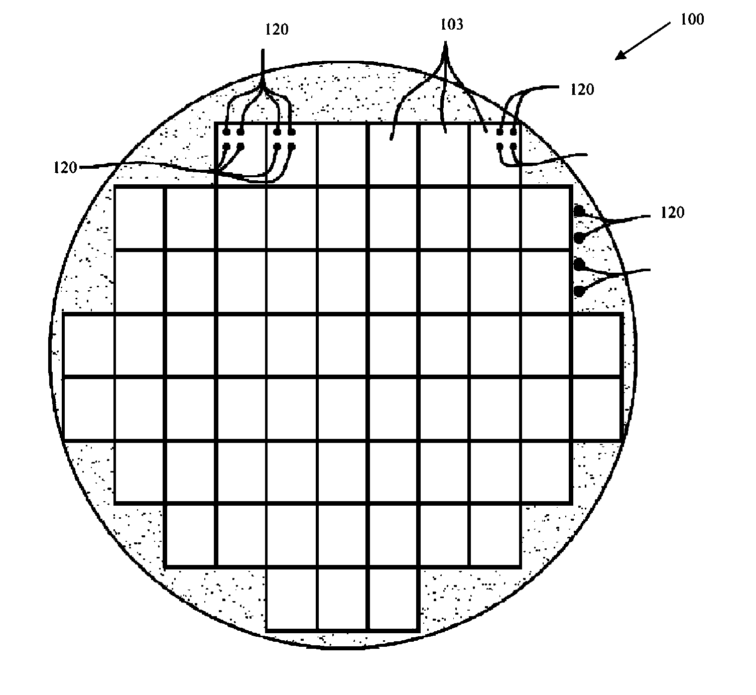
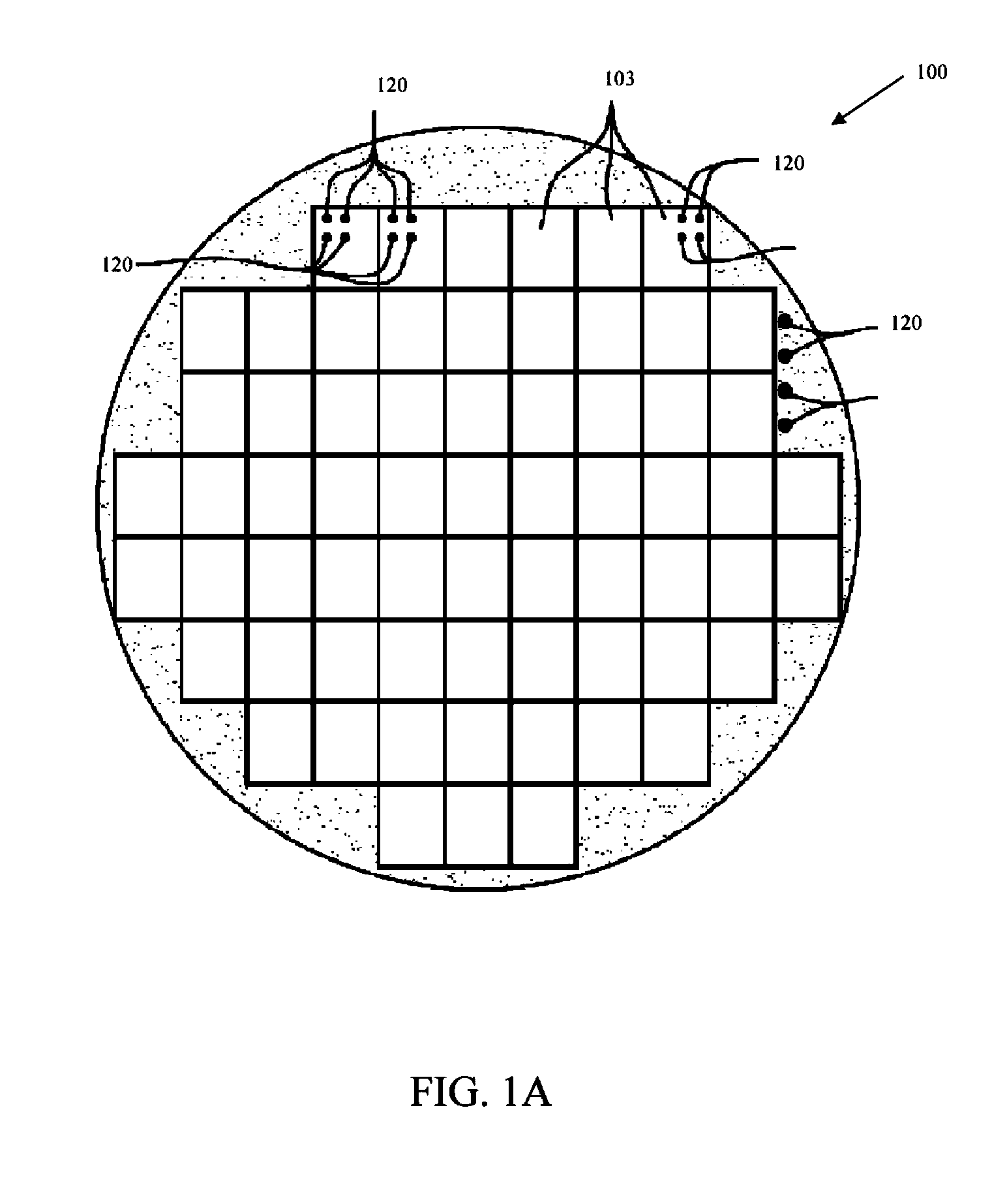
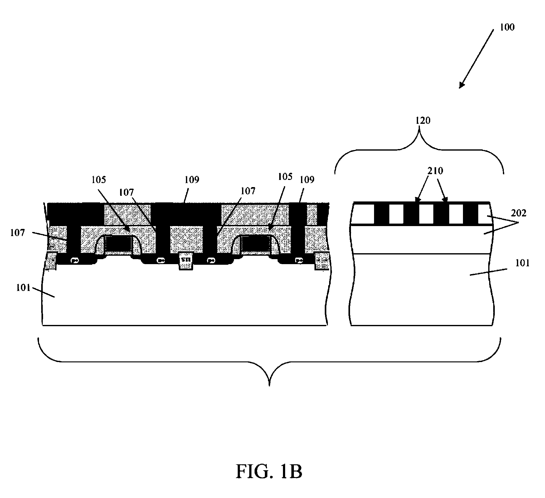
[0025]It was observed that techniques for validating fabrication processes and tools can make use of test structures. The test structures may be fabricated using the same processes as the semiconductor devices, by maki...


PUM


Abstract

There is set forth herein in one embodiment, a structure including a metallic grating having a grating pattern, the metallic grating including a critical dimension. The metallic grating can output a spectral profile when exposed to electromagnetic radiation, the spectral profile having a feature. The grating pattern can be configured so that a change of the critical dimension produces a shift in a value of the feature of the spectral profile. A method can include propagating input electromagnetic radiation onto a metallic grating having a two dimensional periodic grating pattern and measuring a critical dimension of the metallic grating using output electromagnetic radiation from the metallic grating.

Description

CROSS REFERENCE TO RELATED APPLICATIONS[0001]This application claims the benefit of priority of U.S. Provisional App. No. 62 / 047,626 entitled “METALLIC GRATINGS AND MEASUREMENT METHODS THEREOF” filed Sep. 8, 2014, which is incorporated herein by reference in its entirety. International Patent App. No. ______ (Attorney Docket No. 2835.038AWO) entitled “METALLIC GRATINGS AND MEASUREMENT METHODS THEREOF” filed on Sep. 8, 2015 is incorporated by reference herein in its entirety.FIELD[0002]The present disclosure relates to gratings and measurement methods using gratings, and more particularly to metallic gratings and measurement methods using metallic gratings.BACKGROUND[0003]Over the past several decades, the semiconductor industry has continued to increase semiconductor device density by reducing critical dimensions of device structures, such as transistors. During the fabrication of semiconductor devices, structures must be fabricated within specified tolerances of their critical dime...

Claims


Application Information

Patent Timeline
IPC IPC(8): G01N21/21G01B11/02G01N21/95
CPCG01N21/211G01B11/02G01N2201/0683G01N2021/213G01N21/9501G01N21/956G01N21/25
Inventor O'MULLANE, SAMDIEBOLD, ALAIN C.PETERSON, BRENNANKELLER, NICHOLAS
Owner THE RES FOUND OF STATE UNIV OF NEW YORK
Why Eureka
Try Eureka