Eureka AIR delivers breakthrough ideas for toughest innovation challenges, trusted by R&D personnel around the world.

Sensor chip, detection method, and detection apparatus

Active Publication Date: 2016-03-17
PANASONIC CORP
View PDF2 Cites 4 Cited by
  • Summary
  • Abstract
  • Description
  • Claims
  • Application Information

AI Technical Summary

Benefits of technology

The patent text describes a problem where sensor chips embedded in subjects are easily damaged due to contact with the embedding jig and the subject. As a result, the sensor sensitivity and life inside the subject are reduced. The solution proposed in the patent is to restrain the sensor chip from being damaged when embedded inside a subject, which allows for more accurate detection of analytes such as glucose.

Problems solved by technology

Since the metal pattern layer is composed of minute structures of metal, it has poor physical durability.
Therefore, when the aforementioned sensor chip is embedded inside a subject, due to contact between the sensor plane and the specialized embedding jig, and further due to contact between the sensor plane and the subject (e.g., biological tissue), the metal minute structures may be destroyed.
This has resulted in the problem of a reduced sensor sensitivity and a shorter sensor life inside the subject.

Method used


Image

  • Sensor chip, detection method, and detection apparatus
  • Sensor chip, detection method, and detection apparatus
  • Sensor chip, detection method, and detection apparatus

Examples


embodiment 1

[0033]Embodiment 1 will be described with reference to FIG. 6.

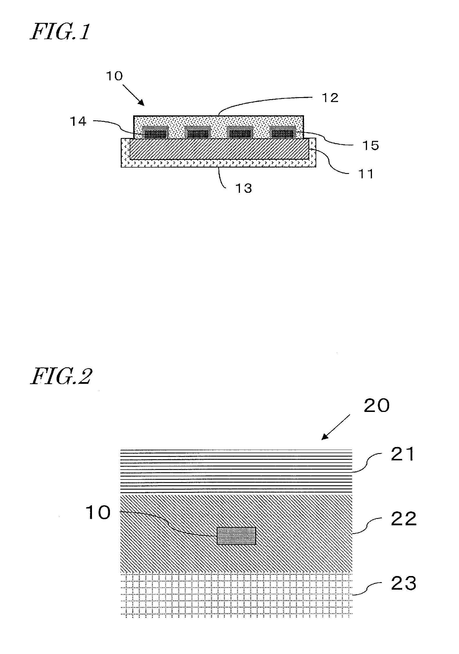
[0034]FIG. 6 is a diagram showing a sensor chip 110 according to Embodiment 1. The sensor chip 110 of Embodiment 1 is a sensor chip which detects an analyte inside a subject. The sensor chip 110 may be embedded in the subject.

[0035]The sensor chip 110 includes a substrate 111, a metal pattern 114, a proximate substance 115, and a light shielding layer 112. The metal pattern 114 is provided on the substrate 111. The metal pattern 114 induces a surface plasmon wave by being irradiated with excitation light.

[0036]The proximate substance 115 is provided on or near the metal pattern 114. When irradiated with excitation light, the proximate substance 115 generates first surface-enhanced Raman-scattered light having a first peak. The first surface-enhanced Raman-scattered light does not vary with changes in the concentration of the analyte.

[0037]Moreover, the proximate substance 115 is a substance that binds to the analyte. When...

embodiment 2

[0045]Embodiment 2 will be described with reference to FIG. 1 to FIG. 5, and FIG. 7. In Embodiment 2, an analyte detection method by using the sensor chip 110 described in Embodiment 1 is proposed.

[0046]Embodiment 2 illustrates the sensor chip 10 shown in FIG. 1 as a typical example of the sensor chip 110. Embodiment 2 illustrates a biological body as the subject. Embodiment 2 illustrates glucose as the analyte. Moreover, a phenylboronic acid compound is illustrated as the proximate substance. In Embodiment 2, a light scattering layer is illustrated as the light shielding layer.

[0047]FIG. 7 is an illustrative flowchart of the detection method according to Embodiment 2. The detection method of Embodiment 2 includes steps (a) to (g) as described below. With the detection method of Embodiment 2, by utilizing scattered light from the proximate substance, it can be determined whether the light shielding layer has been degraded inside the subject or not. In doing so, obtaining a second in...

embodiment 3

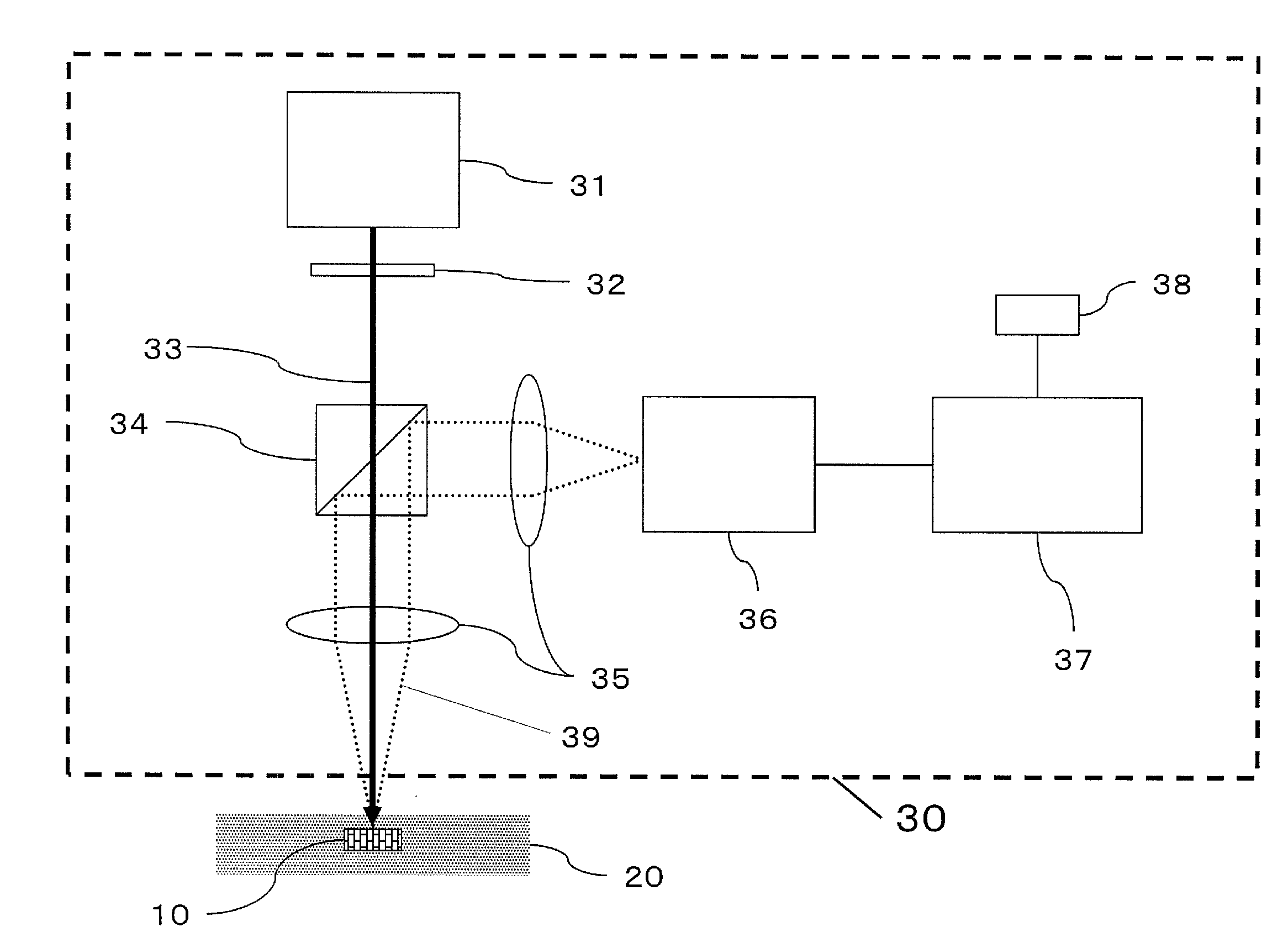
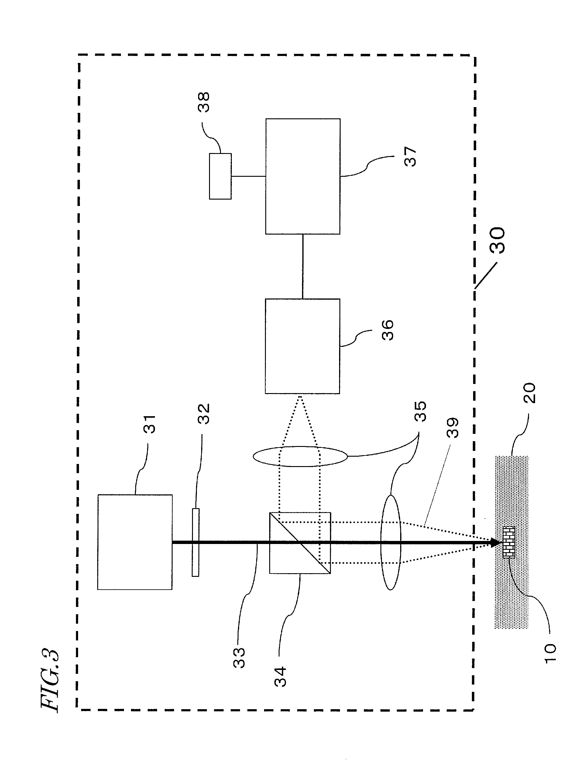
[0104]Embodiment 3 will be described with reference to FIG. 8. In Embodiment 3, a detection apparatus for detecting an analyte by using the sensor chip 110 described in Embodiment 1 is proposed.

[0105]FIG. 8 is a diagram showing a detection apparatus 130 according to Embodiment 3. The detection apparatus 130 of Embodiment 3 is a detection apparatus which detects an analyte by using the sensor chip 110 described in Embodiment 1. The detection apparatus 130 includes a light source 131 which emits excitation light, a detection section 140 which detects scattered light, and a calculation section 137.

[0106]The detection apparatus 130 irradiates the sensor chip 110, which is e.g. embedded inside a subject 200, with excitation light from the light source 131 to generate first surface-enhanced Raman-scattered light. The detection apparatus 130 detects the generated first surface-enhanced Raman-scattered light with the detection section 140, thereby obtaining a first intensity Xa.

[0107]At thi...


PUM


Abstract

An exemplary sensor chip includes a substrate, a metal pattern, a proximate substance, and a light shielding layer. The metal pattern is on the substrate. The proximate substance is on or near the metal pattern. The light shielding layer is provided on the substrate so as to cover the metal pattern and the proximate substance. The light shielding layer is a layer that blocks the excitation light from going into the proximate substance, and is made of a substance which becomes degraded inside a subject.

Description

[0001]This is a continuation of International Application No. PCT / JP2014 / 002832, with an international filing date of May 28, 2014, which claims priority of Japanese Patent Application No. 2013-117587, filed on Jun. 4, 2013, the contents of which are hereby incorporated by reference.BACKGROUND[0002]1. Technical Field[0003]The present application relates to a sensor chip, a detection method, and a detection apparatus for detecting an analyte based on surface-enhanced Raman spectroscopy.[0004]2. Description of the Related Art[0005]In Raman spectroscopy, a substance is irradiated with monochromatic light (excitation light) of a certain frequency so that scattered light occurs therefrom, and any scattered light that has a different frequency (hereinafter referred to as Raman-scattered light) from the frequency of the incident light is spectroscopically detected. A difference (Raman shift) between the frequency of the Raman-scattered light and the frequency of the incident light is equal...

Claims


Application Information

Patent Timeline
IPC IPC(8): A61B5/1459G01N21/65
CPCG01N21/658A61B5/1459A61B5/0075A61B5/14532G01N21/554
Inventor OKUMURA, YASUAKIKAWAMURA, TATSUROUMINAMIGUCHI, MASARUSHIOI, MASAHIKO
Owner PANASONIC CORP
Why Eureka
Eureka Blog
Learn More