Semiconductor memory device having count value control circuit

a memory device and control circuit technology, applied in the field of semiconductor memory devices, can solve the problems of data loss, data loss in memory cells, and data loss in memory cells, and achieve the effect of preventing data loss, preventing data loss, and preventing data loss

Inactive Publication Date: 2016-03-17
MICRON TECH INC
View PDF0 Cites 75 Cited by
  • Summary
  • Abstract
  • Description
  • Claims
  • Application Information

AI Technical Summary

Benefits of technology

[0012]According to various embodiments of the present invention, an additional refresh can be performed on a memory cell with degraded informatio

Problems solved by technology

Since a DRAM (Dynamic Random Access Memory), which is a typical semiconductor memory device, stores information with electric charges accumulated in a cell capacitor, the information is lost unless a refresh operation is regularly performed.
However data storing abilitie

Method used


Image

  • Semiconductor memory device having count value control circuit
  • Semiconductor memory device having count value control circuit
  • Semiconductor memory device having count value control circuit

Examples


first embodiment

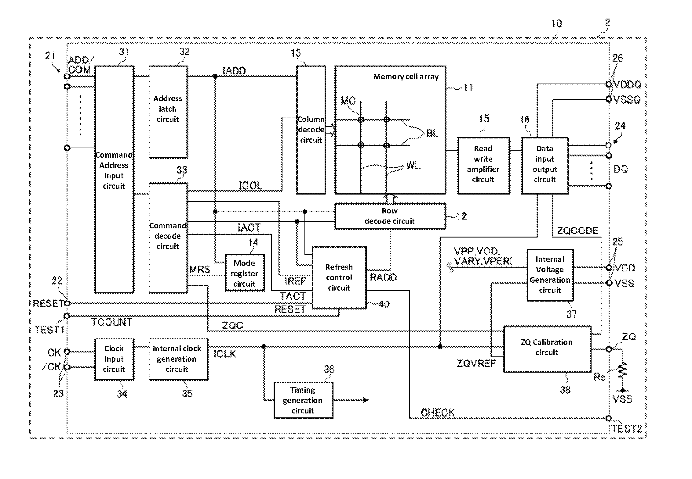
[0063]FIG. 4 is a circuit diagram of the refresh control circuit 40 according to the first embodiment.

[0064]As depicted in FIG. 4, the refresh control circuit 40 according to the first embodiment includes a refresh counter 41, an access count portion 50, an address generation portion 60, and a selection circuit 42.

[0065]The refresh counter 41 is a circuit which generates a row address (refresh address) RADDa to be refreshed in response to a refresh signal IREF. The refresh address RADDa indicating a count value of the circuit is updated (incremented or decremented) in response to the refresh signal IREF. For this reason, if a refresh command is issued a plurality of times (for example, 8 k times) so that the count value of the refresh counter 41 goes around once in a period of one refresh cycle, all word lines WL can be refreshed in the period of one refresh cycle. However, when the select signal SEL is activated, the count value is not updated even if the refresh signal IREF is inp...

first structure example

[0084]In a first structure example, only the test active signal TACT is used, and the count set signal TCOUNT is not necessary. To check the operation of the address generation portion 60, any of the detection signals MAX is required to be activated. However, if the setting is such that the detection signal is activated when the count value of the counting circuit reaches a maximum value of 65535, the same word line WL has to be accessed 65535 times. In the operation test, such a large amount of memory accesses in order to check the function of the address generation portion 60 is burdensome.

[0085]To avoid such a burden, in the first structure example, when the access counter control circuit 52 receives the test active signal TACT, the count values of the counting circuits 510 to 51p included in the access counter 51 are all set at a predetermined test value (a first value). In the case in which the detection signal MAX is activated when the count value of each counting circuit reac...

second structure example

[0086]Also in a second structure example, only the test active signal TACT is used, and the count set signal TCOUNT is not necessary. In the second structure example, the access counter control circuit 52 retains the test value in advance. In the second structure example, when the access counter control circuit 52 receives the test active signal TACT, the count value of the counting circuits 510 to 51p included in the access counter 51 are all set at the internal test value. Unlike the first structure example, any value can be set to the counting circuits 510 to 51p, and therefore it is effective at checking the operation of each of the counting circuits 510 to 51p.


PUM


Abstract

A device includes a data storing cell array including a plurality of groups of data storing cells each configured to be accessed responsive to the input of the corresponding one of the row addresses and a count value control circuit coupled to each of the groups of the data storing cells. The count value control circuit is configured to update a count value stored in each of the groups of data storing cells by a first value responsive to the input of the corresponding one of the row addresses in a first operation mode and to set the count value stored in each of the groups of the data storing cells to a second value responsive to the input of the corresponding one of the row addresses in a second operation mode.

Description

[0001]This application is based upon and claims the benefit of priority from Japanese patent application No. 2013-231671 filed on Nov. 8, 2013, the disclosure of which are incorporated herein in its entirely by reference.BACKGROUND[0002]1. Field of the Invention[0003]This invention relates to a semiconductor device, in particular, a semiconductor device that includes a data storing cell array including a plurality groups of data storing cells each configured to be accessed in response to the input of the corresponding one of the row addresses.[0004]2. Description of the Related Art[0005]Since a DRAM (Dynamic Random Access Memory), which is a typical semiconductor memory device, stores information with electric charges accumulated in a cell capacitor, the information is lost unless a refresh operation is regularly performed. Therefore, from a control device which controls a DRAM, a refresh command for making an instruction for a refresh operation is regularly issued, as described in ...

Claims


Application Information

Patent Timeline
IPC IPC(8): G11C7/22G11C11/406G11C11/408G11C11/4096G11C11/418G11C11/419
CPCG11C7/22G11C11/419G11C11/418G11C11/408G11C11/4096G11C11/406G11C7/109G11C11/4076G11C11/4087G11C11/4093G11C29/022G11C29/028G11C29/50016
Inventor FUJIWARA, TAKAYUKIOISHI, KANJIISHIKAWA, SHIN
Owner MICRON TECH INC
Why Eureka
Try Eureka