Circuit board

a technology of circuit boards and soldering holes, applied in the field of circuit boards, can solve the problems of insufficient bonding strength, short circuit between adjacent terminals and terminals, insufficient connection areas between solder and power supply terminals, and insufficient connection areas between solder and ground terminals, so as to reduce the risk of short circuit between terminals arranged at a small pitch and increase the efficiency of power supply to an electronic component connected to the circuit board by flip-chip bonding

Active Publication Date: 2016-03-31
NGK SPARK PLUG CO LTD
View PDF6 Cites 3 Cited by
  • Summary
  • Abstract
  • Description
  • Claims
  • Application Information

AI Technical Summary

Benefits of technology

[0009]The present invention has been made in light of the above-described problem, and an object of the present invention is to provide a circuit board with which the risk of short-circuiting

Problems solved by technology

If the pitch of the signal terminals arranged in the same opening formed in the solder resist layer is small, there is a risk that solder will flow between the adjacent terminals and the terminals will be short-circuited.
In addition, when only the lower surfaces of the fine signal terminals are bonded to the underlying resin insulating layer, there is a risk that the bonding strength will be insufficient.
If these terminals are all provided with the above-described reinforc

Method used


Image

  • Circuit board
  • Circuit board
  • Circuit board

Examples


Embodiment Construction

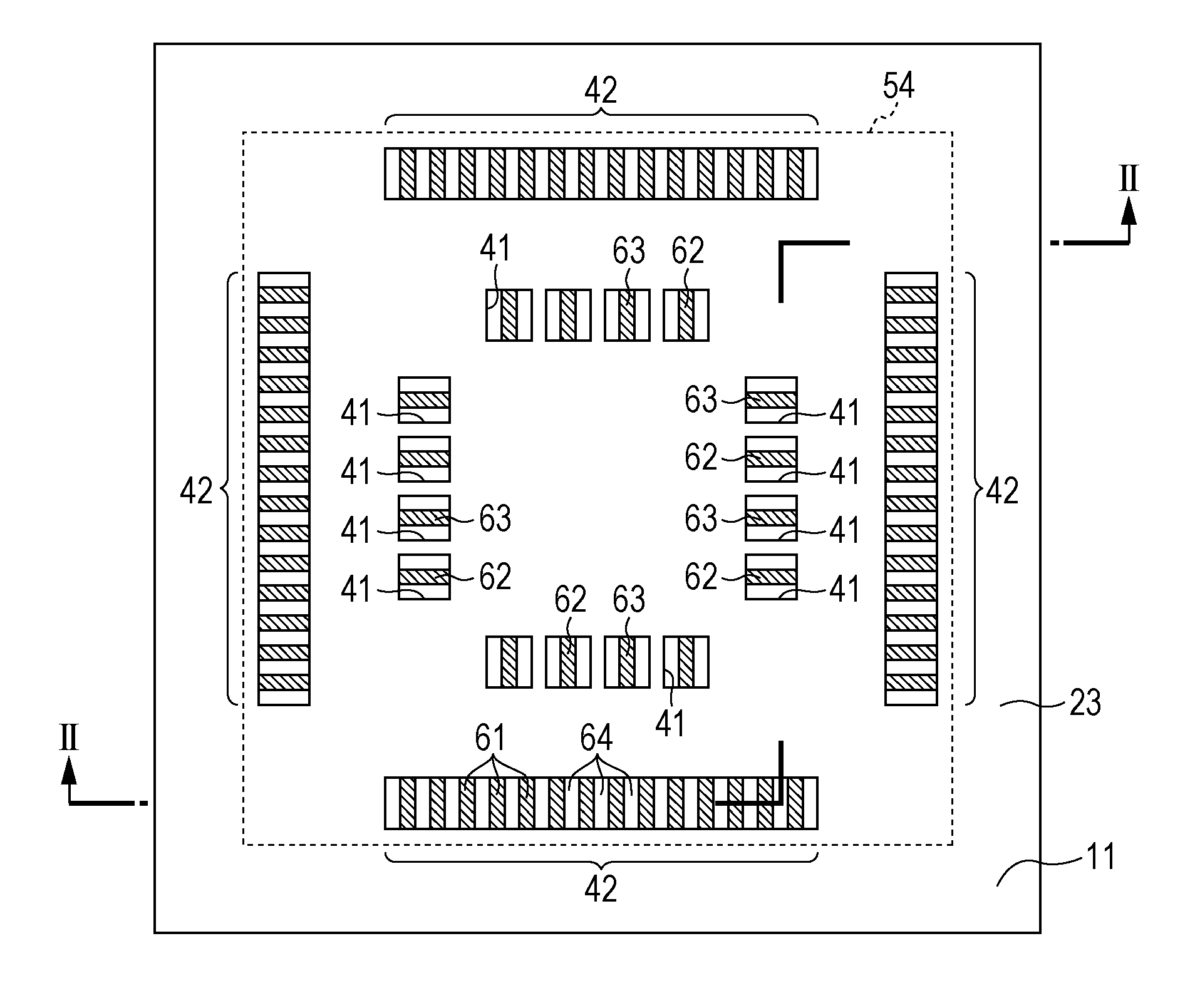
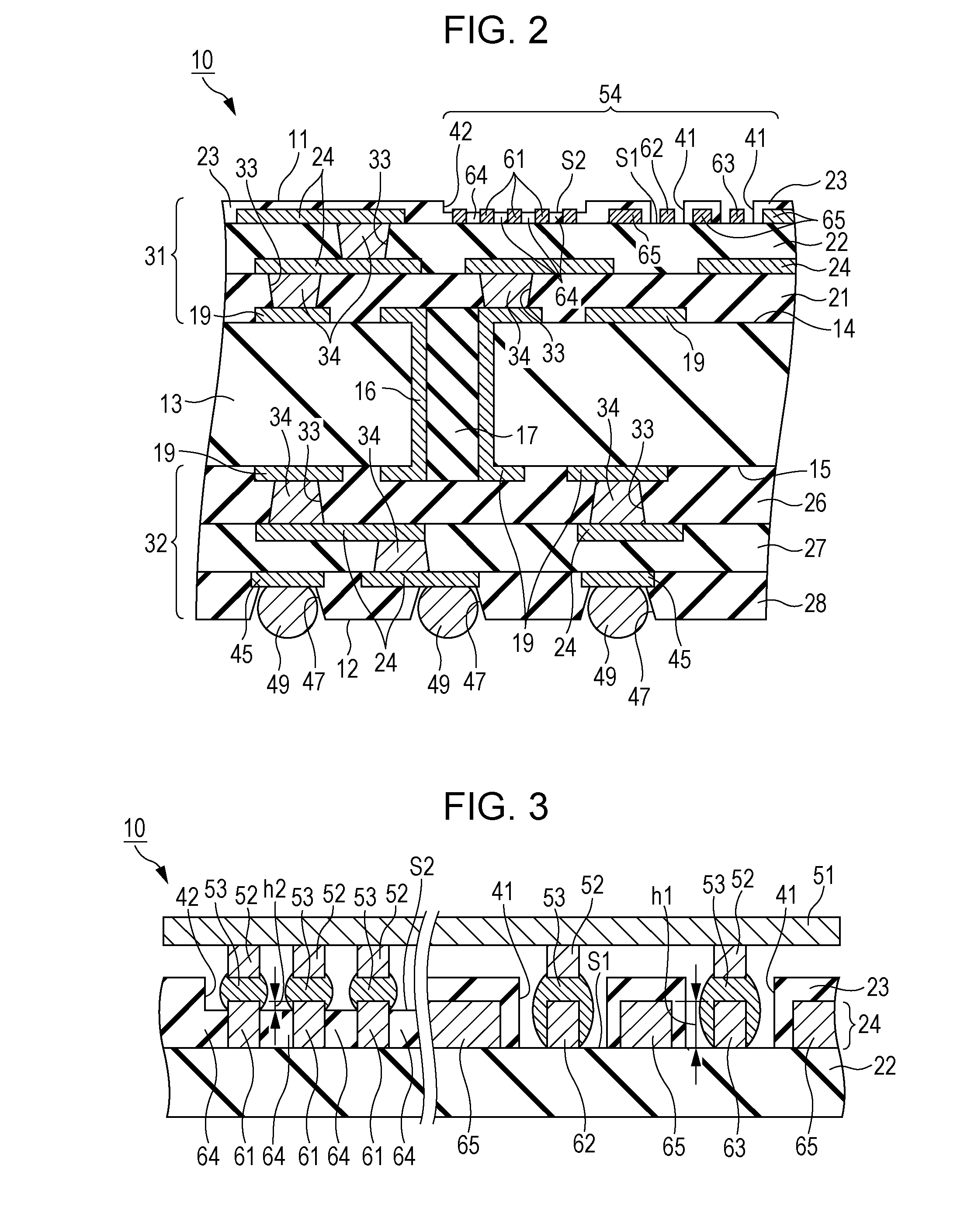
[0043]An organic circuit board will be described in detail below with reference to FIGS. 1 to 14 as a circuit board according to an embodiment of the present invention.

[0044]As illustrated in FIGS. 1 to 3, an organic circuit board 10 according to the present embodiment is a circuit board having a peripheral-type structure, and includes a board principal surface 11, which serves as an IC-chip mounting surface, and a board back surface 12 that opposes the principal surface 11. The organic circuit board 10 includes a rectangular plate-shaped core substrate 13, a first build-up layer 31 formed on a core principal surface (upper surface in FIG. 2) of the core substrate 13, and a second build-up layer 32 formed on a core back surface 15 (lower surface in FIG. 2) of the core substrate 13.

[0045]The core substrate 13 according to the present embodiment is made of, for example, a resin insulating material (glass epoxy material) obtained by impregnating glass cloth, which serves as a reinforci...


PUM


Abstract

A circuit board is provided that includes an outermost conductor layer including a plurality of terminals for flip-chip bonding and an outermost resin insulating layer defining a first opening and a second opening in an electronic-component mounting region. One of a power supply terminal and a ground terminal is exposed in the first opening. A plurality of signal terminals are exposed in the second opening. The resin insulating layer includes a reinforcing portion that defines an inner bottom surface of the second opening. A height of a portion of the terminal exposed in the first opening, the portion projecting from an inner bottom surface of the first opening, is greater than a height of portions of the terminals exposed in the second opening, the portions projecting from the inner bottom surface of the second opening.

Description

CROSS REFERENCE TO RELATED APPLICATIONS[0001]The present application claims priority to Japanese Patent Application No. 2014-199366, which was filed on Sep. 29, 2014, the disclosure of which is herein incorporated by reference in its entirety.BACKGROUND OF THE INVENTION[0002]1. Field of the Invention[0003]The present invention relates to a circuit board including a plurality of terminals to which an electronic component, such as an integrated circuit (IC) chip, is connected by flip-chip bonding.[0004]2. Description of the Related Art[0005]Semiconductor integrated circuit devices (IC chips) used as microprocessors of computers or the like generally include many external connection terminals on the bottom surface thereof. In particular, IC chips having many signal terminals arranged along the outer periphery of the bottom surface thereof are called peripheral-type IC chips. Terminals to which the terminals on the IC chips are to be connected by flip-chip bonding are provided on a prin...

Claims


Application Information

Patent Timeline
IPC IPC(8): H05K1/11H05K1/02H05K1/03
CPCH05K1/11H05K1/0313H05K1/0298H01L2224/16225H05K1/111H05K3/3436H05K3/3452H05K3/4069H05K3/4644Y02P70/50
Inventor NAGAI, MAKOTOMORI, SEIJIITO, TATSUYA
Owner NGK SPARK PLUG CO LTD
Why Eureka
Try Eureka