
Capacitive touch device and excitation signal generating circuit and method thereof

a capacitive touch and excitation signal technology, applied in the direction of instruments, computing, electric digital data processing, etc., can solve the problems of high manufacturing cost, higher power consumption of excitation signal generator, and large size touch panel with more sensing traces, etc., to solve signal distortion, solve high power consumption, and simple circuit structure

Inactive Publication Date: 2016-04-07
ELAN MICROELECTRONICS CORPORATION
View PDF3 Cites 6 Cited by
  • Summary
  • Abstract
  • Description
  • Claims
  • Application Information

AI Technical Summary

Benefits of technology

The present invention provides an excitation signal generating circuit with a simple circuit structure and a method of generating the excitation signal. The circuit directly generates the PDM signal as an excitation signal output to the sensing traces without the need for amplifiers, which simplifies the circuit structure, reduces manufacturing costs, and lowers power consumption. The PDM signal passes through a current transmission path, which acts as a low pass filter, to recover an available analog sensing signal with low signal distortion and increased accuracy of current sensing signals. The capacitive touch device using the excitation signal generating circuit also provides the same benefits. The generating method generates the PDM signal with the same frequency as the excitation signal, which is directly output to the sensing traces where it is recovered to an analog excitation signal. The technical effects of the present invention include reduced signal distortion, increased accuracy of current sensing signals, and lower power consumption.

Problems solved by technology

Therefore, the excitation signal generator has higher power consumption and also increases manufacturing cost for a larger size touch panel with more sensing traces.

Method used


Image

  • Capacitive touch device and excitation signal generating circuit and method thereof
  • Capacitive touch device and excitation signal generating circuit and method thereof
  • Capacitive touch device and excitation signal generating circuit and method thereof

Examples


Embodiment Construction

[0040]The present invention provides an improved excitation signal generating circuit of a capacitive touch device to simplify the circuit structure thereof.

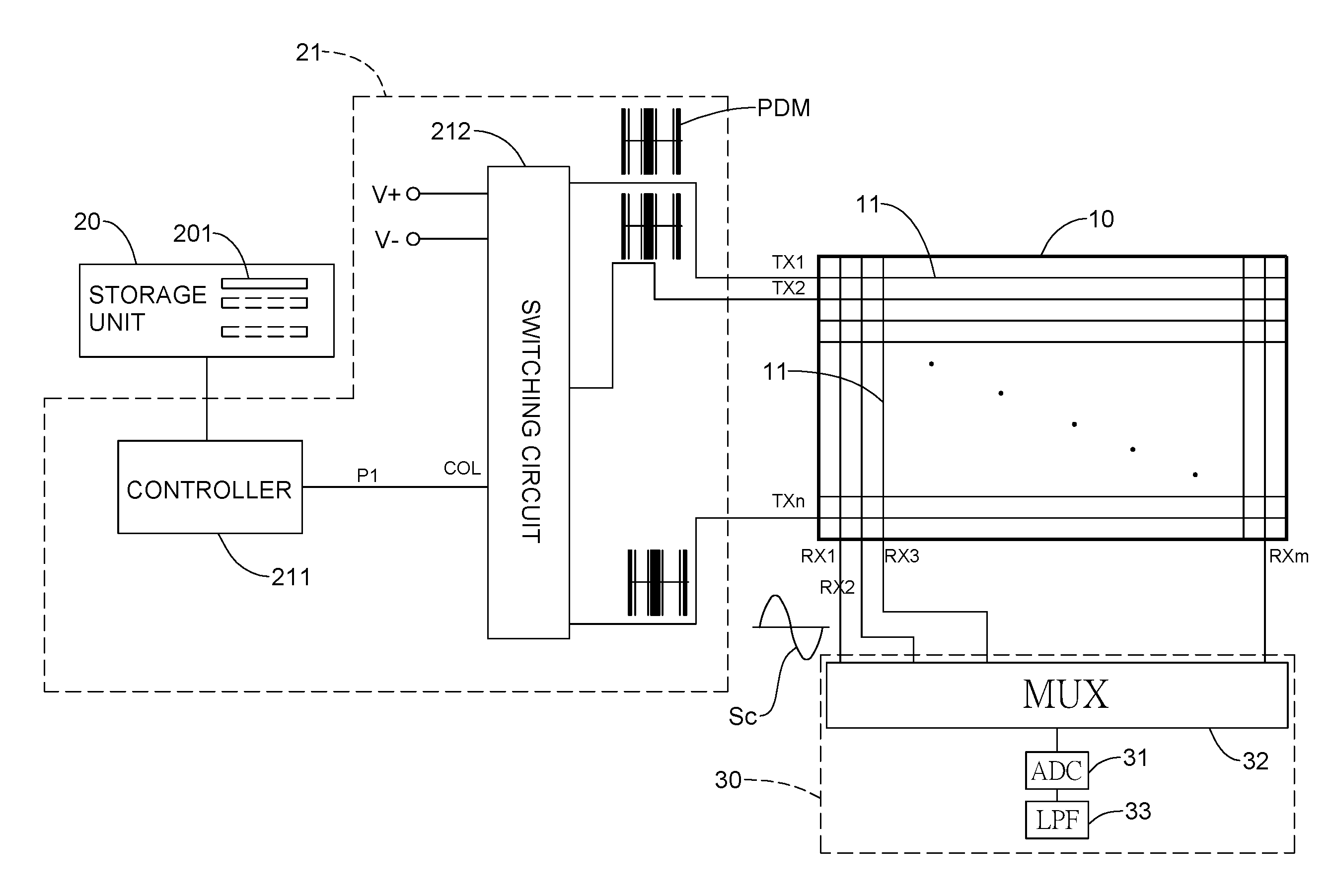
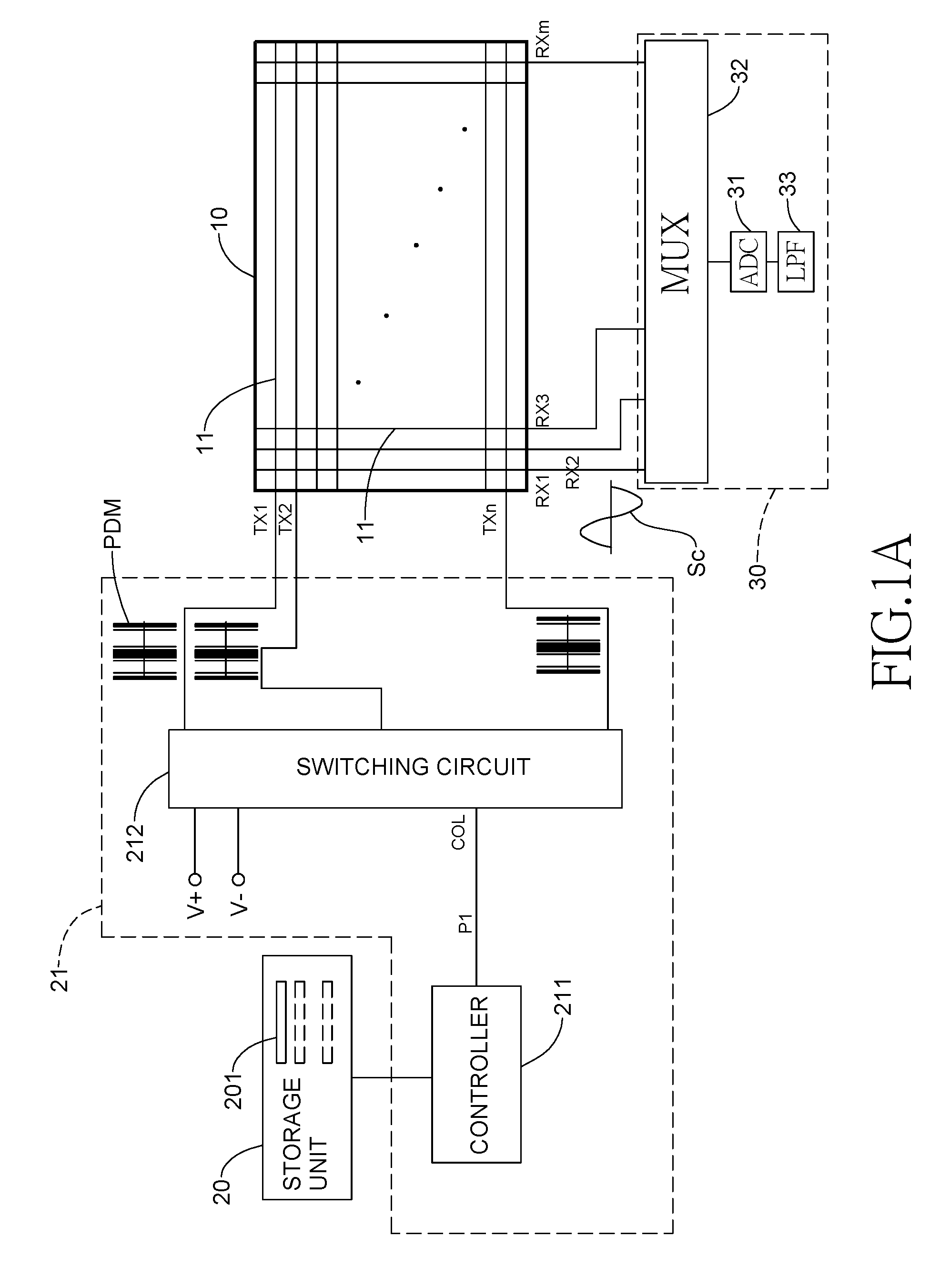
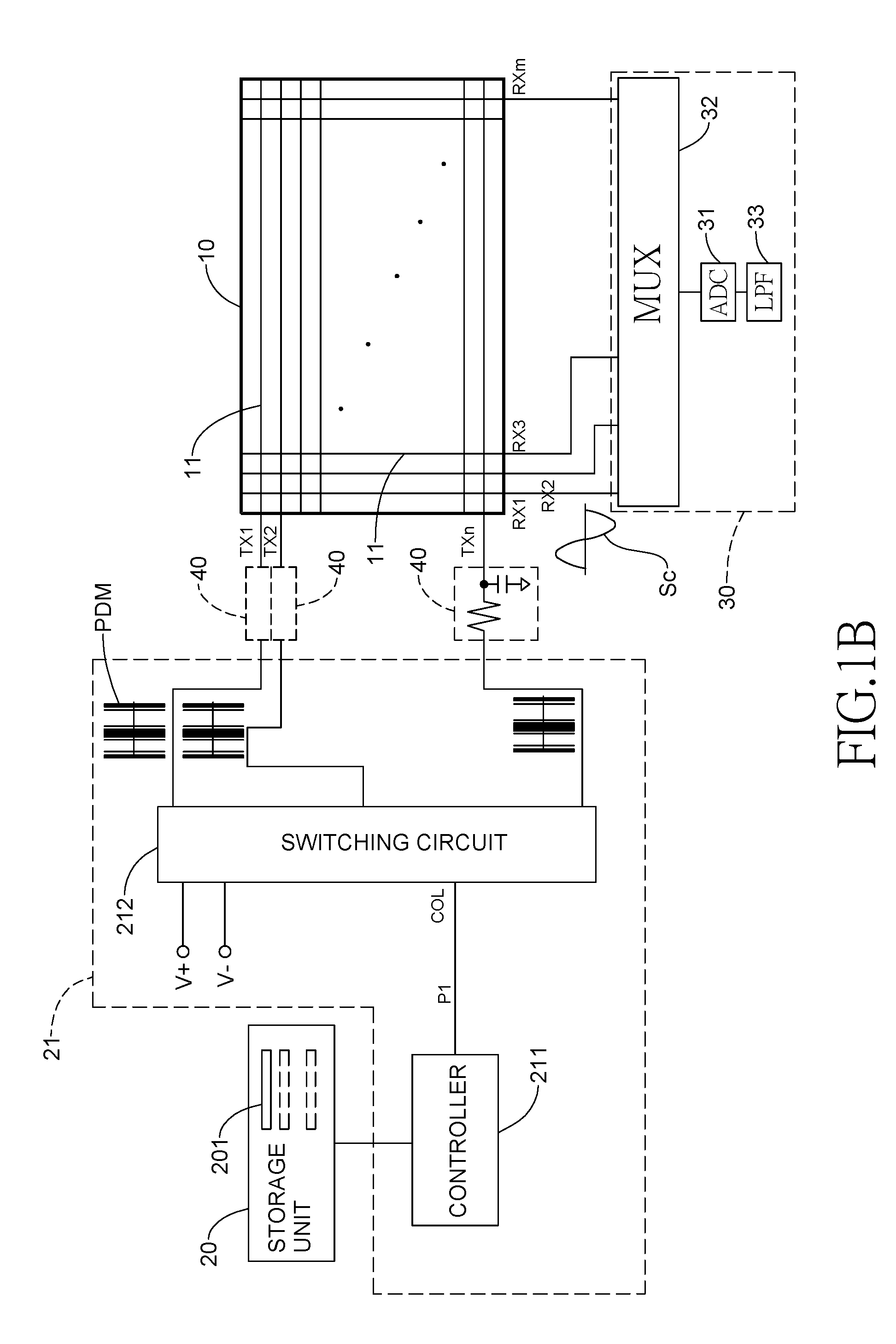
[0041]With reference to FIG. 1A, a capacitive touch device of a first preferred embodiment of the present invention has a touch panel 10, an excitation signal generating circuit (not numbered) and a receiving circuit 30.

[0042]The touch panel 10 has multiple sensing traces 11 including multiple first axis sensing traces and a second axis sensing traces crossing the first axis sensing traces. In the first preferred embodiment, a mutual-capacitive scanning method is used as an example so the first axis sensing traces are used as driving traces TX1˜TXn and the second axis sensing traces are used as sensing traces RX1˜RXm. If a self-capacitive scanning method is used, each sensing trace is used as the driving and receiving trace.

[0043]The excitation signal generating circuit has a storage unit 20 and a pulse density modulation (herei...


PUM


Abstract

The present invention is related to a capacitive touch device and excitation signal generating circuit and method thereof. The excitation signal generating circuit is connected to multiple sensing traces of the capacitive touch device, and has a storage unit storing at least one set of digital data. Each set of digital data is corresponding to a frequency. The PDM signal generator reads the set of digital data and converts the read set of digital data to a PDM signal according to the frequency of the read set of digital data. The PDM signal is recovered to an analog excitation signal since the PDM signal passes through a current transmission path, which is equivalent to a low pass filter. Therefore, the present invention can decrease a distortion of the sensing signal to increase accuracy of the sensing signal and to save power.

Description

CROSS-REFERENCE TO RELATED APPLICATIONS[0001]This application is based upon and claims priority under 35 U.S.C. 119 from Taiwan Patent Application No. 103134173 filed on Oct. 1, 2014, which is hereby specifically incorporated herein by this reference thereto.BACKGROUND OF THE INVENTION[0002]1. Field of the Invention[0003]The present invention is related to a capacitive touch device, and more particularly to an excitation signal generating circuit and method of the capacitive touch device.[0004]2. Description of the Prior Arts[0005]A conventional capacitive touch device has a touch panel and a scanning circuit. The touch panel has multiple sensing traces, and the scanning circuit provides an excitation signal to parts or all of the sensing traces in sequence. A charging current is generated on the sensing trace to which the excitation signal is supplied based on the influence of capacitance effect. After a period of charging time, the charging current on the sensing trace is stable. ...

Claims


Application Information

Patent Timeline
Patent Type & Authority Applications(United States)
IPC IPC(8): G06F3/044
CPCG06F3/044G06F3/04166G06F3/0446
Inventor LIN, CHIA-HSINGCHEN, HAN-WEICHEN, JYUN-YU
Owner ELAN MICROELECTRONICS CORPORATION
Learn More