Semiconductor device and battery monitoring system

Active Publication Date: 2016-04-28
LAPIS SEMICON CO LTD
View PDF0 Cites 0 Cited by
  • Summary
  • Abstract
  • Description
  • Claims
  • Application Information

AI Technical Summary

Benefits of technology

[0015]According to the present invention, with the semiconductor device, it is possible to

Problems solved by technology

According to the conventional technology described above, when the power consumption of one of the conventional battery monitoring semiconductor devices supplying the power voltage is increased, the power consumption of the assembled batteries may exceed that of the other of the conventional battery monitoring semiconductor devices.
Accordingly, a voltage balance among the assembled batteries may become unstable, thereby causing a fluctuation in the voltage of the assembled batteries.
When the one of the conventional battery monitoring semiconductor devices communicates with the control unit, the power consumptio

Method used


Image

  • Semiconductor device and battery monitoring system
  • Semiconductor device and battery monitoring system
  • Semiconductor device and battery monitoring system

Examples


Example

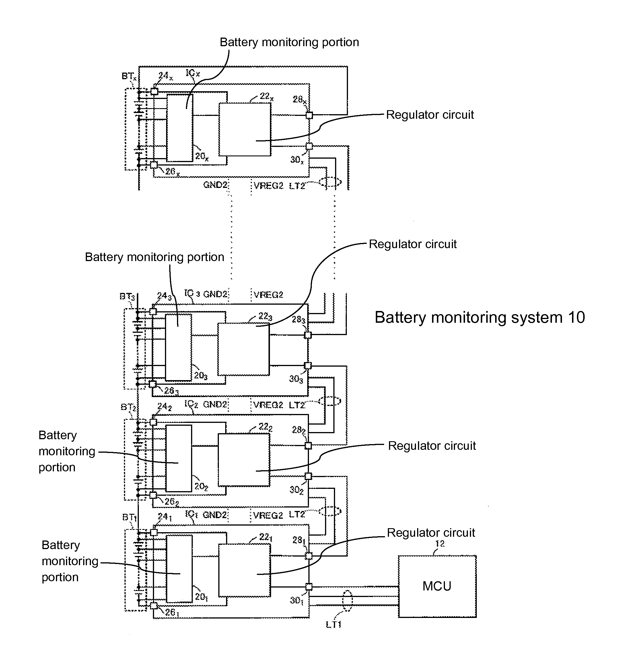
[0023]A first embodiment of the present invention will be explained. FIG. 1 is a block diagram showing a configuration of a battery monitoring system 10 according to the first embodiment of the present invention.

[0024]As shown in FIG. 1, the battery monitoring system 10 includes assembled batteries BT1 to BTx in the number of x (x is a natural number greater than one); battery monitoring ICs (Integrated Circuit) IC1 to ICx in the number of x; and an MCU (Memory Control Unit) 12. It should be noted that, in the following description, the assembled batteries and the battery monitoring ICs are collectively referred to as the assembled batteries BT and the battery monitoring ICs IC, respectively. When it is necessary to differentiate each of the assembled batteries BT and the battery monitoring ICs IC, a specific number or symbol (1 to x) is attached to the legend (IC or BT).

[0025]In the first embodiment, each of the assembled batteries BT includes a plurality of battery cells. It shoul...

Example

Second Embodiment

[0078]A second embodiment of the present invention will be explained next. When the battery monitoring system 10 includes the battery monitoring ICs IC at a plurality of states, each of the battery monitoring ICs IC may includes a setting portion for setting the product of the mirror ratios (k×n×m), that is the electrical current ratio of each transistor.

[0079]FIG. 6 is a circuit diagram showing a configuration of the battery monitoring IC (Integrated Circuit) of the battery monitoring system 10 in which the setting portion is provided for setting the mirror ratios according to the second embodiment of the present invention.

[0080]As shown in FIG. 6, in addition to the configuration of the battery monitoring ICs IC in the first embodiment (refer to FIG. 3), each of the battery monitoring ICs IC includes a register 50 and a decoder 52 that function as the setting portion. It is configured such that the MCU (Memory Control Unit) 12 transmits an instruction to the regis...


PUM


Abstract

A semiconductor device includes a first electrical current source connected to an assembled battery through a power source terminal; and a second electrical current source connected to an input terminal to which an external electrical current is input. The first electrical current source is configured to generate a first electrical current according to a reference voltage based on a power source electrical current input into the power source terminal, and to output the first electrical current to an output terminal. The second electrical current source is configured to generate a second electrical current according to the reference voltage based on the external electrical current, and to output the second electrical current to the output terminal.

Description

BACKGROUND OF THE INVENTION AND RELATED ART STATEMENT[0001]The present invention relates to a semiconductor device and a battery monitoring system.[0002]According to a conventional technology, a plurality of battery cells is connected in series to constitute an assembled battery for generating a high voltage. In general, a conventional battery monitoring semiconductor device is provided for measuring and monitoring a battery voltage of the battery cells of the assembled battery.[0003]A conventional battery monitoring system formed of the conventional battery monitoring semiconductor devices, for example, may include a plurality of assembled batteries, and the conventional battery monitoring semiconductor devices are connected in a daisy chain arrangement for monitoring each of the assembled batteries. The conventional battery monitoring system may further include a control unit for controlling each of the conventional battery monitoring semiconductor devices.[0004]In the conventiona...

Claims


Application Information

Patent Timeline
IPC IPC(8): H02J7/00
CPCH02J2007/0067H02J7/0063H01M10/4257H01M10/4285H01M2010/4271H02J7/00714H01M10/482Y02E60/10
Inventor YANAGAWA, KENJI
Owner LAPIS SEMICON CO LTD
Why Eureka
Try Eureka