Liquid crystal array substrate, electronic device, and method for testing liquid crystal array substrate

a liquid crystal array and substrate technology, applied in the field of substrates, can solve the problems of color distortion, difficult to test whether the pixels of the main region and the sub-region are short-circuited, and the panel of the lc electronic device is degraded or scrapped

Active Publication Date: 2016-05-05
TCL CHINA STAR OPTOELECTRONICS TECH CO LTD
View PDF1 Cites 7 Cited by
  • Summary
  • Abstract
  • Description
  • Claims
  • Application Information

AI Technical Summary

Benefits of technology

[0019]The electronic device and the over-voltage protection circuit of the present invention capable of executing over-voltage protection quickly when the electronic device is worked at the 2D mode or the 3D mode.

Problems solved by technology

In the multi-angle display mode, because LC molecules are pointed to different directions when viewing at different viewing angles, which causes a color distortion when viewing at a large viewing angle.
However, for the pixel with the LCS design, it is hard to test whether pixels of the main region and the sub-region are short-circuited, namely is unqualified by using common method.
Thus causing panels of the LC electronic device is degraded or is scrapped.

Method used


Image

  • Liquid crystal array substrate, electronic device, and method for testing liquid crystal array substrate
  • Liquid crystal array substrate, electronic device, and method for testing liquid crystal array substrate
  • Liquid crystal array substrate, electronic device, and method for testing liquid crystal array substrate

Examples


Embodiment Construction

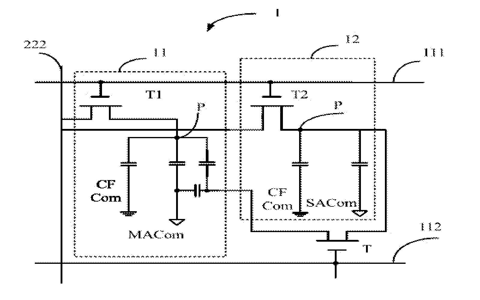
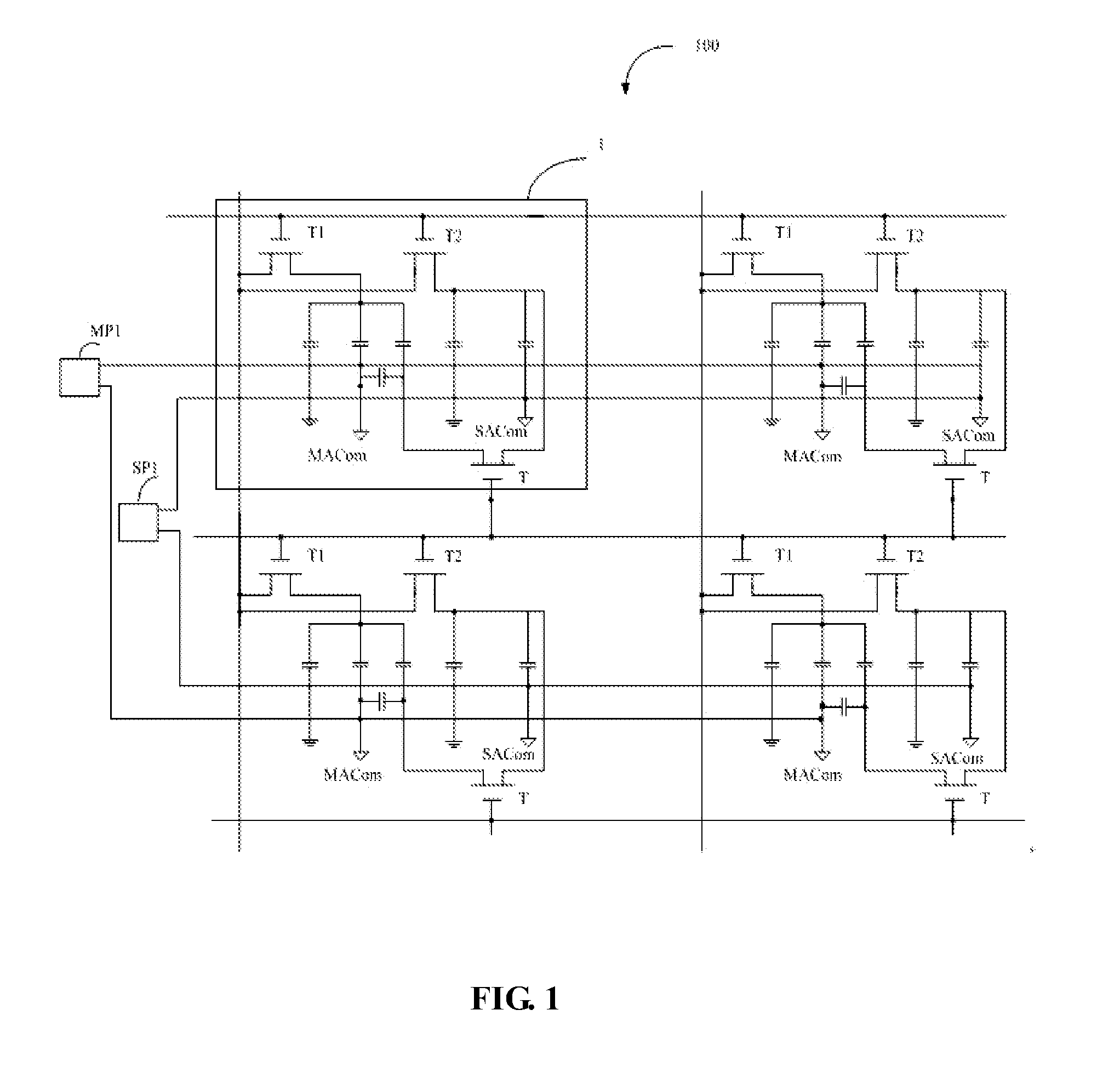
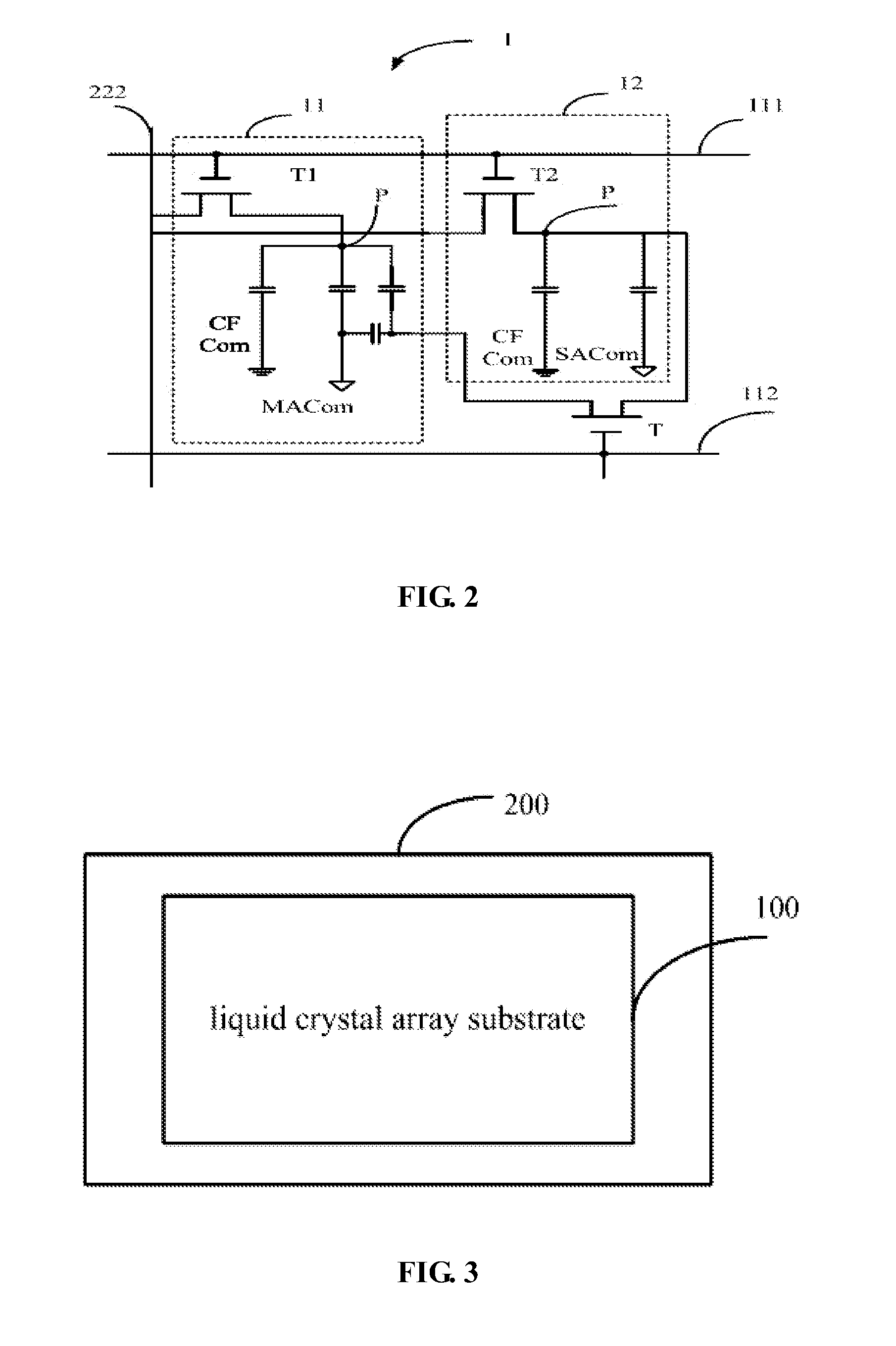
[0024]Referring to FIGS. 1 and 2 together, FIG. 1 is a schematic diagram of a liquid crystal (LC) array substrate 100, FIG. 2 is a schematic diagram of a pixel region 1 included by the LC array substrate 100. In the embodiment, the LC array substrate 100 has the low color shift (LCS) design. The LC array substrate 100 includes a number of pixel region 1 arranged in array mode. The pixel region 1 includes a main region 11, a sub-region 12, and an adjustment thin film transistor (TFT) T. The main region 11 includes a first TFT T1 and a main region array common electrode lead wire MAcom. The sub-region 12 includes a second TFT T2 and a sub-region array common electrode lead wire SAcom. The adjustment TFT T is used to adjust a ratio of voltage of the main region 11 and the sub-region 12, thus achieving the LCS design.

[0025]Gates of the first TFT T1 and the second TFT T2 of each pixel region 1 are connected to a first scan line 111. Sources of the first TFT T1 and the second TFT T2 of ea...


PUM

PropertyMeasurementUnit
voltageaaaaaaaaaa
conductiveaaaaaaaaaa
color distortionaaaaaaaaaa

Abstract

A liquid crystal (LC) array substrate includes a number of pixel regions, each pixel region includes a main region, a sub-region, and an adjustment thin film transistor (TFT), the adjustment TFT adjusts a ratio of voltage of the main region and the sub-region to achieve a LCS design. The main region comprises a first TFT and a main region array common electrode lead wire, the sub-region comprises a second TFT and a sub-region array common electrode lead wire, and the main region array common electrode lead wire and the sub-region array common electrode lead wire are electrically isolated. The main region array common electrode lead wire of all pixel regions of the LC array substrate are connected to a main region conductive pad, the sub-region array common electrode lead wire of all pixel regions of the LC array substrate are connected to a sub-region conductive pad.

Description

TECHNICAL FIELD OF THE INVENTION[0001]The present invention relates to substrates, and more particularly, to a liquid crystal array substrate and an electronic device with the same, and a method for testing the liquid crystal array substrate.BACKGROUND OF THE INVENTION[0002]Nowadays, liquid crystal (LC) electronic device, such as liquid crystal display (LCD) and LCD television are more popular. A common LC electronic device usual has a multi-angle display mode. In the multi-angle display mode, because LC molecules are pointed to different directions when viewing at different viewing angles, which causes a color distortion when viewing at a large viewing angle. Usually, in order to improve the color distortion, one pixel of the LC molecule is divided to two parts when designing pixel region of the LC molecules, one part is a main region, and the other is a sub-region. The color distortion is improved by controlling voltage of the two regions. Therein, the design of dividing the pixel...

Claims


Application Information

Patent Timeline
Patent Type & Authority Applications(United States)
IPC IPC(8): G02F1/1362G02F1/1343G02F1/1368
CPCG02F1/136286G02F1/1368G02F1/134309G02F2001/136254G09G3/3659G09G2300/0447G09G2300/0852G09G2330/08G02F1/1309G02F1/13624G02F1/134345G02F1/136254
Inventor YAO, XIAOHUIHSU, JE HAO
Owner TCL CHINA STAR OPTOELECTRONICS TECH CO LTD
Why Eureka
Try Eureka