Apparatus for testing semiconductor integrated circuit

Inactive Publication Date: 2006-06-06
RENESAS ELECTRONICS CORP
View PDF8 Cites 60 Cited by
  • Summary
  • Abstract
  • Description
  • Claims
  • Application Information

AI Technical Summary

Benefits of technology

[0009]The invention proposes an improved apparatus for testing a semiconductor integrated circuit which enables easy expansion of capability to test a

Problems solved by technology

However, in association with a recent fast progression of an on-chip system, the scale of digital circuitry to be incorporated into an analog LSI becomes larger.
Hence, testing of the analog LSI through use of the conventional testing capability becomes difficult.
Further, an increase in the time required for testing is also feared.
Moreover, preparation of a mixed-signal-type tester for a consolidated-type LSI is also conceivable, which requires big-budget investments for a special tester.
Analogous problems arise in a cust

Method used


Image

  • Apparatus for testing semiconductor integrated circuit
  • Apparatus for testing semiconductor integrated circuit
  • Apparatus for testing semiconductor integrated circuit

Examples


Example

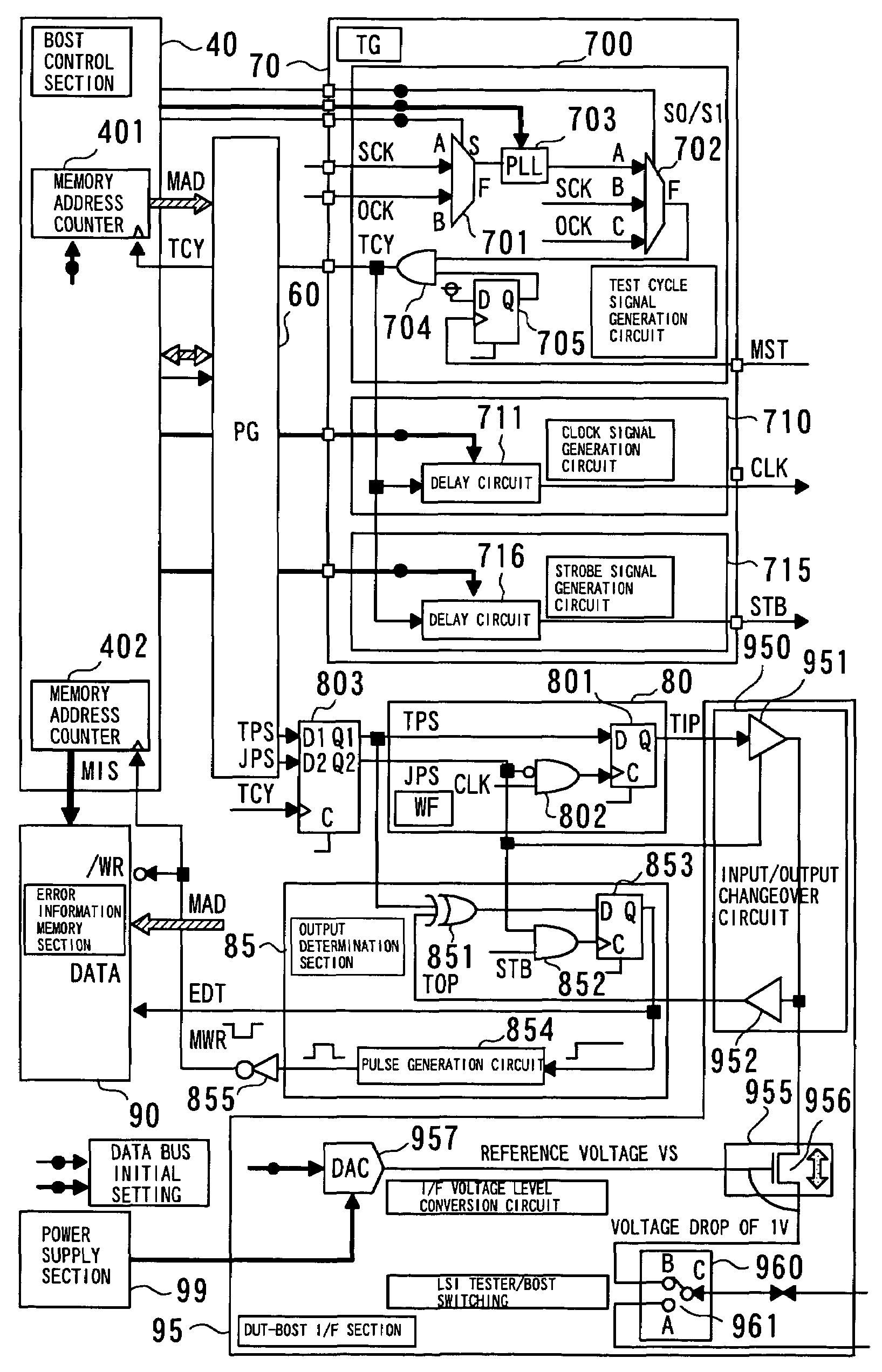
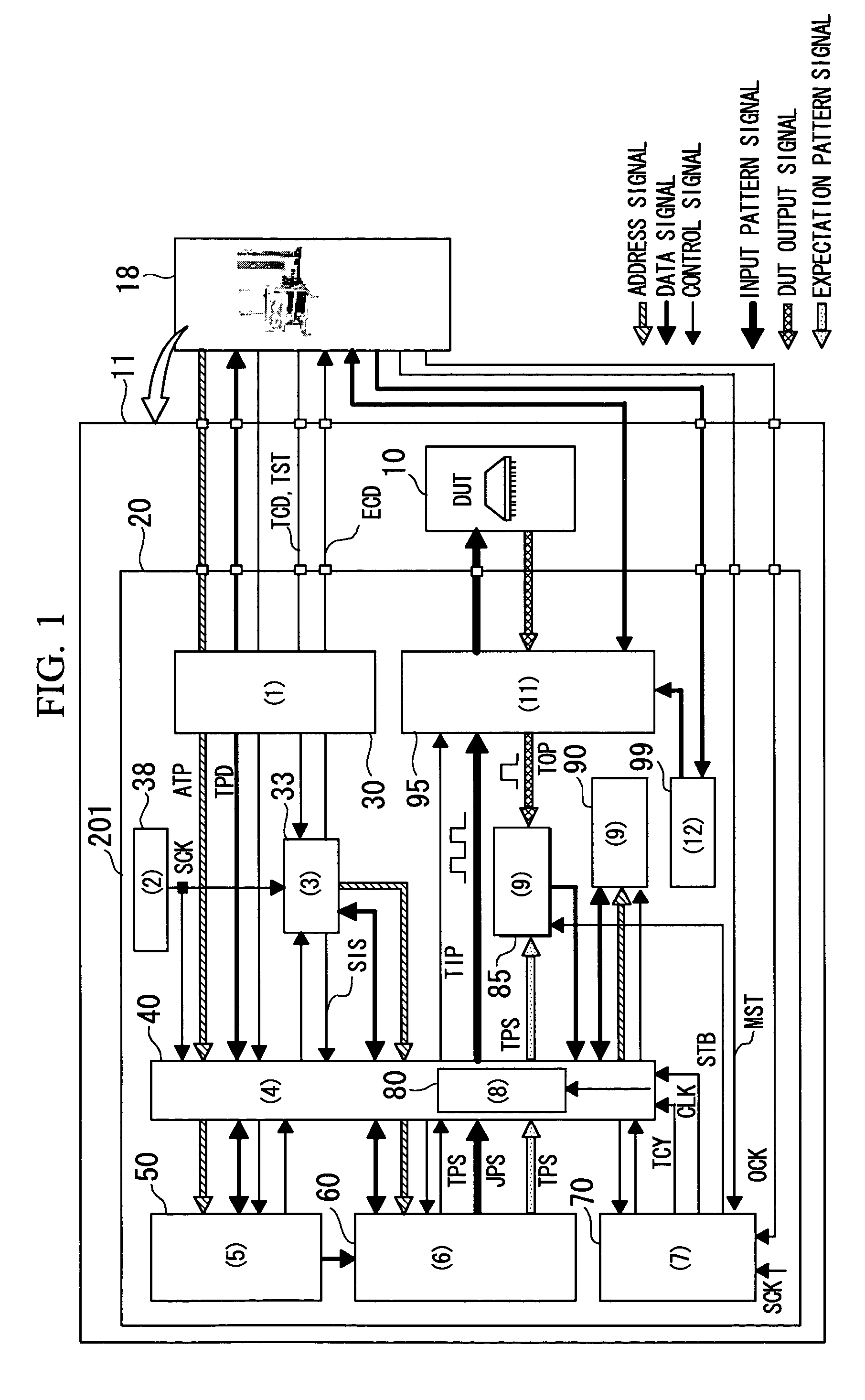
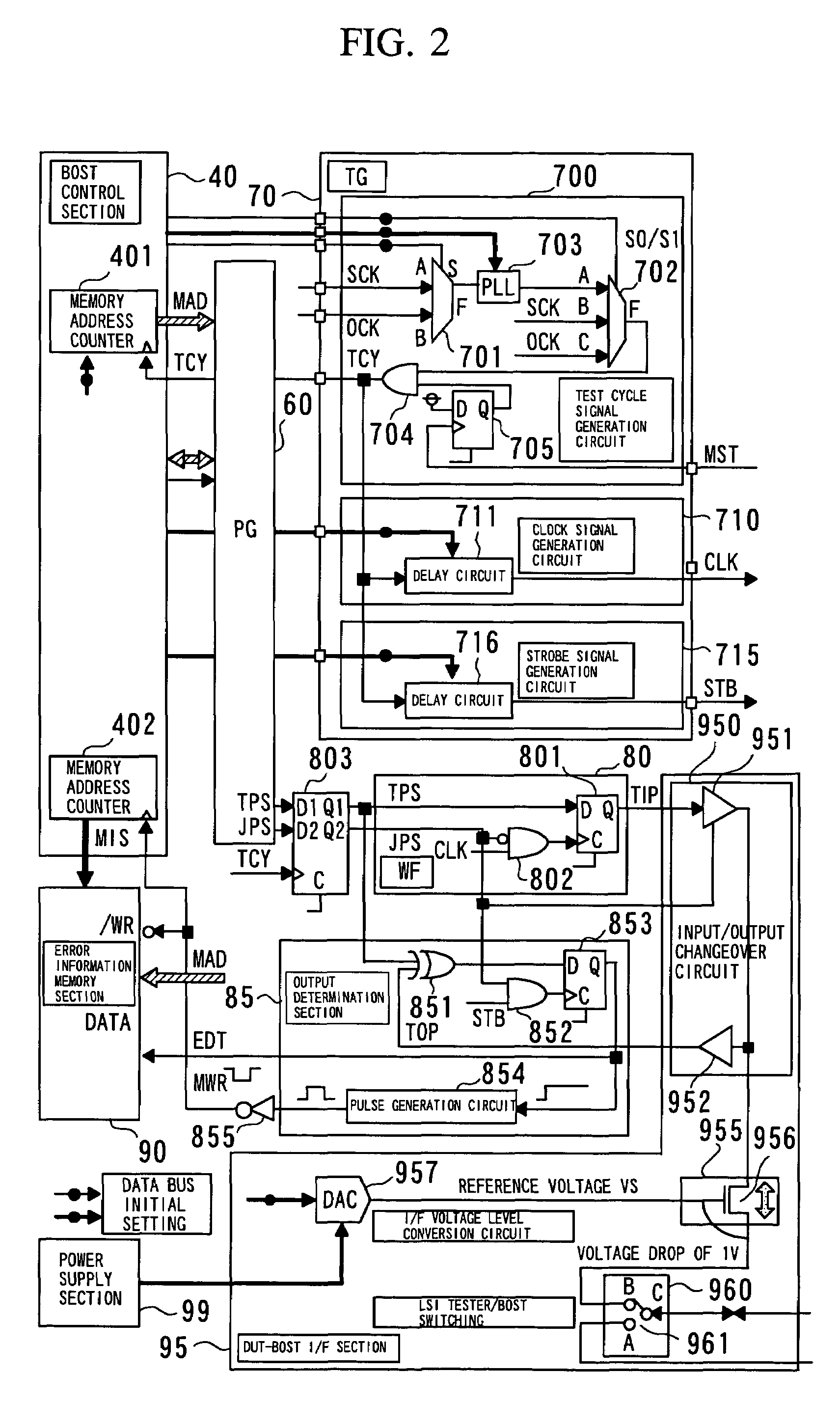
[0069]FIG. 1 is a block diagram showing a circuit configuration of a first embodiment of an apparatus for testing a semiconductor integrated circuit according to the invention. FIG. 2 is a block diagram showing a circuit configuration of an ancillary test device of the first embodiment. FIG. 3 is a timing chart showing a test operation of the first embodiment.

[0070]The overall circuit configuration of the first embodiment will now be described by reference to FIG. 1. An apparatus for testing a semiconductor integrated circuit of the first embodiment is for testing a semiconductor integrated circuit 10 under test and has a test circuit board 11, an external tester 18, and an ancillary test device 20. The semiconductor integrated circuit 10 under test is also called a DUT (Device Under Test). Various types of LSIs are applicable to the DUT 10. The first embodiment is based on the assumption of a consolidated-type LSI formed by incorporating a digital circuit; specifically, a logic cir...

Example

Embodiment 1-1

[0140]Embodiment 1-1 is an embodiment of implementation of the apparatus for testing a semiconductor integrated circuit according to the invention. Embodiment 1-1 has a BOST assembly 210A constituting the BOST device 20. The BOST assembly 210A is formed by combination of five circuit boards 211 through 215.

[0141]FIG. 4A is a conceptual rendering of the configuration of the boards of the BOST assembly 210A, and FIG. 4B is a perspective external view of the BOST assembly 210A.

[0142]The BOST assembly 210A of embodiment 1-1 is disposed on a DUT board 110 and formed by combination of five circuit boards 211, 212, 213, 214, and 215. The two circuit boards 211, 212 are disposed in parallel with the DUT board 110, and three circuit boards 213, 214, and 215 are disposed perpendicular to the DUT board 110. The circuit board 211 is disposed at a position immediately above the DUT board 110, and the circuit board 212 is disposed on the circuit board 211. The circuit boards 213, 21...

Example

Embodiment 1-2

[0146]Embodiment 1-2 is an embodiment pertaining to the apparatus for testing a semiconductor integrated circuit of the invention. Embodiment 1-2 has a BOST assembly 210B which is more simplified than the BOST assembly 210A described in connection with embodiment 1-1. FIG. 5 shows a developed view of the BOST assembly 210B of embodiment 1-2. FIG. 5A is a front view showing the basic configuration of the BOST assembly 210B: FIG. 5B is a side view showing the circuit boards 213, 214, and 215; FIG. 5C is a block diagram of an angle connector; and FIG. 6 is a side view showing a specific configuration of the BOST assembly 210B.

[0147]First, as shown in FIG. 5A, the circuit boards 213, 214, and 215 are rectangular boards that are slightly elongated in the vertical direction, and straight-type connectors CN2, CN3 to be used for connecting together the circuit boards 213, 214, and 215 are provided at front and back upper ends of the respective circuit boards 213, 214, and 215....


PUM


Abstract

An apparatus for testing a semiconductor integrated circuit has a test circuit board and an ancillary test device. The ancillary test device can test a digital circuit. The ancillary test device has test pattern memory, a test pattern signal generator, and a control section for controlling an operation for the test pattern data selected from among the plurality of test pattern data sets stored in the test pattern memory and an operation for writing the selected test pattern data into the test pattern signal generator. The ancillary test device generates a test input pattern signal on the basis of test pattern data written in the test pattern signal generator and determines a test output pattern signal output from the semiconductor integrated circuit on the basis of the test input pattern signal, thereby testing a digital circuit.

Description

BACKGROUND OF THE INVENTION[0001]1. Field of the Invention[0002]The invention relates to an apparatus for testing a semiconductor integrated circuit, the apparatus having an ancillary test device placed in the vicinity of a test circuit board which exchanges signals with a semiconductor integrated circuit under test.[0003]2. Background Art[0004]A large-scale analog semiconductor integrated circuit (hereinafter called an “LSI”) is usually tested through use of an analog-only tester. The analog-only tester is configured so as to supply a test input signal to a semiconductor integrated circuit under test (hereinafter called a “DUT”) by way of a test circuit board which exchanges signals with the DUT and receives a test output signal from the DUT and analyzes the output signal. However, in relation to a recent semiconductor integrated circuit, the number of consolidated-type LSIs; that is, a combination of an analog LSI having digital circuitry, more specifically, a combination of an an...

Claims


Application Information

Patent Timeline
IPC IPC(8): G01R31/28G06F11/00G01R31/316G01R31/3183G01R31/319G06F11/263G11C29/56
CPCG01R31/31905G01R31/31919G11C29/56G06F11/263G01R31/31926
Inventor MORI, HISAYAFUNAKURA, TERUHIKOHANAI, HISAYOSHI
Owner RENESAS ELECTRONICS CORP
Why Eureka
Try Eureka