Display device and scanning circuit testing method

Active Publication Date: 2005-06-21
SHARP KK
View PDF7 Cites 10 Cited by
  • Summary
  • Abstract
  • Description
  • Claims
  • Application Information

AI Technical Summary

Benefits of technology

[0020]A main object of the present invention is to provide a display device and a scanning circuit testing method therefor, w

Problems solved by technology

However, such a testing method is bound to a problem in that the S/N ratio and the accuracy of testing suffer as the pixel capacitance becomes smaller and the amount of charge read out is reduced, as in a small and fine resolution display device for projection use.
In this case, however, testing needs to be carried out for extended periods of time.
Accordingly, data processing takes time, which lowers testing efficiency.
This inevitably increases the pad area under severe constraints on driver area particularly in small and fine resolution

Method used


Image

  • Display device and scanning circuit testing method
  • Display device and scanning circuit testing method
  • Display device and scanning circuit testing method

Examples


Example

[0054][First Embodiment]

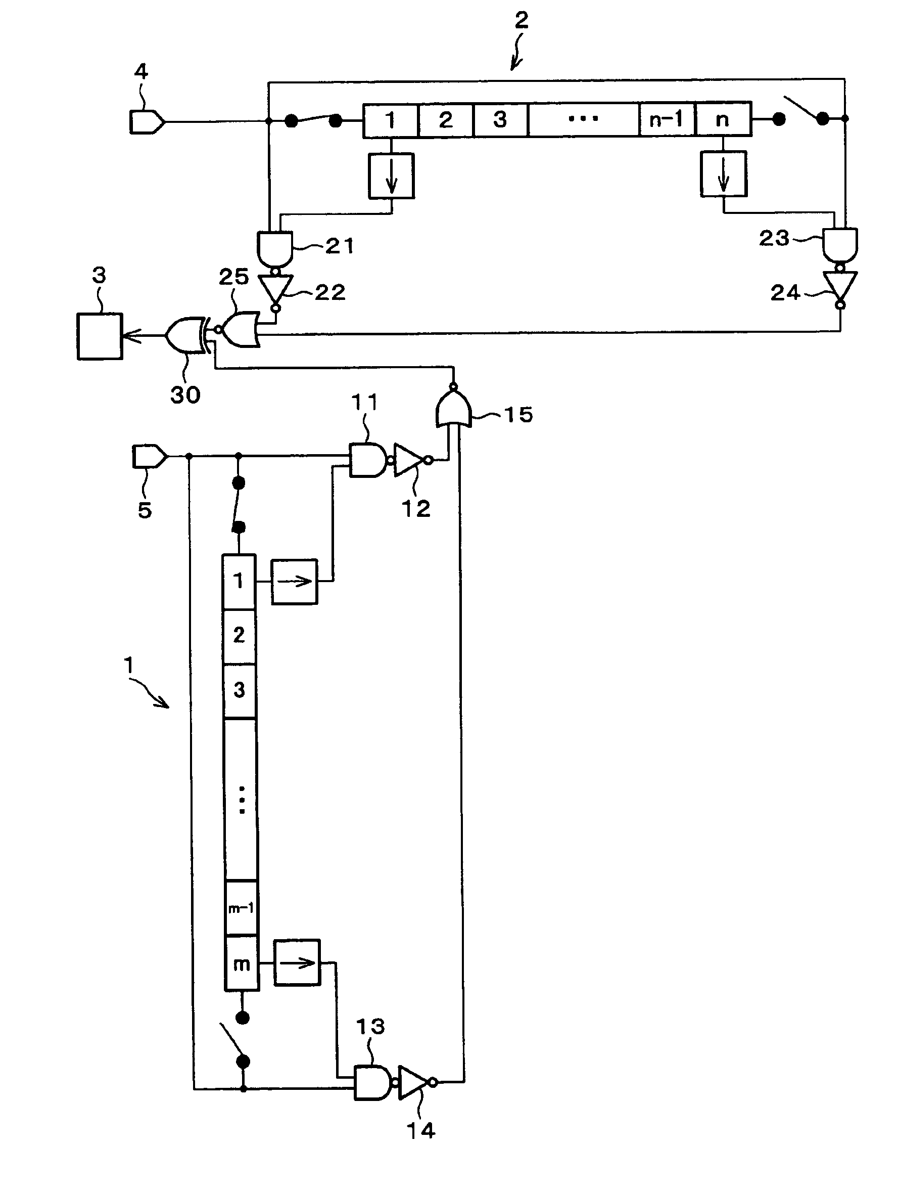
[0055]One embodiment of a display device according to the present invention is described below with reference to FIG. 1 through FIG. 6, and FIG. 9.

[0056]A liquid crystal display device (display device) of the present embodiment includes an active-matrix substrate and a counter substrate, which are disposed face to face via a liquid crystal layer. The liquid crystal display device also includes pixels that are provided in a matrix to make up a pixel array section.

[0057]The active-matrix substrate includes, as shown in FIG. 9, a glass substrate (insulating substrate) 90, thin film transistors (“TFTs” hereinafter) 99, pixel electrodes 92, gate lines, data lines, an interlayer insulating film 94, and auxiliary capacitor wiring (“CS wiring” hereinafter) 93.

[0058]Each TFT 99 is composed of a gate electrode 91 of the gate line, a data electrode of the data line, a channel layer, an gate insulating film 95, a CG-Si film 98, and metal wiring 100.

[0059]On the glass sub...

Example

[0111][Second Embodiment]

[0112]Another embodiment of the present invention is described below with reference to FIG. 7. Note that, constituting elements that are functionally equivalent to those described in the First Embodiment are given the same reference numerals and explanations thereof are omitted here.

[0113]As with the structure shown in FIG. 1 described in the First Embodiment, a liquid crystal display device of the present embodiment has gate and source drivers 1 and 2 that are capable of bi-directional shifting, and input pads 4 and 5, as shown in FIG. 7.

[0114]The gate and source drivers 1 and 2 output signals from the last stages with respect to the shift directions. The output signal of each driver in either shift direction is selected by analog switches in response to input of a scanning direction switching signal.

[0115]The selected output signal is supplied to an EX-OR circuit 76 with or without delay.

[0116]The present embodiment uses three kinds of image display format...

Example

[0126][Third Embodiment]

[0127]Yet another embodiment of the present invention is described below with reference to FIG. 8. Note that, constituting elements that are functionally equivalent to those described in the First Embodiment are given the same reference numerals and explanations thereof are omitted here.

[0128]As with the structure shown in FIG. 1 described in the First Embodiment, a liquid crystal display device of the present embodiment includes gate and source drivers 1 and 2 that are capable of switching shift directions, in addition to a testing pad 3 and input pads 4 and 5, as shown in FIG. 8.

[0129]In response to input of the clock signal G-CK and the start pulse G-SP, the gate driver 1, with its shift direction set in the first direction, shifts the start pulse G-SP as shift data from the first to m-th (last stage of the first direction) stages of the shift registers in synchronism with the clock signal G-CK. Here, a switch 84 is closed and a switch 85 is open. The swit...


PUM


Abstract

Each of a gate driver and a source driver periodically receives a clock signal and a start pulse, where the start pulse has a certain width and is shifted as shift data in the gate driver or source driver in synchronism with the clock signal. A logic circuit composed of an NAND gate and an inverter receives the start pulse and the shift data, the shift data being the output that is supplied after a predetermined delay from the last stage with respect to the shift direction. The output of the inverter is used to test scanning circuits. This provides a display device and a scanning circuit testing method, which enable the scanning circuits to be judged both surely and quickly, without increasing the area or complexity of the circuit.

Description

FIELD OF THE INVENTION[0001]The present invention relates to a display device that is capable of judging an operating state of a scanning circuit. The invention also relates to a scanning circuit testing method for such a display device.BACKGROUND OF THE INVENTION[0002]Conventionally, liquid crystal display devices of a monolithic type, used as a display device, are generally adapted to sample video data via analog switches that are controlled by shift registers.[0003]For example, as shown in FIG. 11(a), the liquid crystal display device includes a pixel capacitor CLC and an auxiliary capacitor Cs that are connected to each pixel in a pixel section, and TFTs (Thin Film Transistors) are provided at the intersections of a plurality of gate lines in the row direction and a plurality of data lines in the column direction. The gate lines are connected to a gate driver and the data lines are connected to a source driver.[0004]Further, counter electrodes are provided opposite the TFTs and ...

Claims


Application Information

Patent Timeline
IPC IPC(8): G01R31/28G01R31/3185G09G3/36G09G3/00G02F1/133G02F1/13G02F1/1345G02F1/167G09F9/00G09G3/20
CPCG01R31/318533G09G3/3648G01R31/318505G09G3/006G09G3/3674Y10S345/904G09G2310/0267G09G2310/0275G09G2310/0283G09G2310/0286G09G2330/12G09G3/3685G11C29/32
Inventor TAKAFUJI, YUTAKASHIRAI, KATSUNORISHIBAZAKI, AKIRA
Owner SHARP KK
Why Eureka
Try Eureka