Blanking aperture array device for multi-beams, and fabrication method of blanking aperture array device for multi-beams
a technology of aperture array and multi-beam, which is applied in the direction of instruments, nuclear engineering, optical elements, etc., can solve the problems of inability to achieve the charge inhibiting effect in the structure, the inability to perfectly inhibit the electrostatic charge of the insulator at the time of beam irradiation, and the distortion or blur of beams
- Summary
- Abstract
- Description
- Claims
- Application Information
AI Technical Summary
Benefits of technology
Problems solved by technology
Method used
Image

Examples
first embodiment
[0018]In a first embodiment of the present invention, there is described a method of fabricating, by a simpler process, a blanking aperture array device that can inhibit surface electrostatic charge generated by multi-beam irradiation.
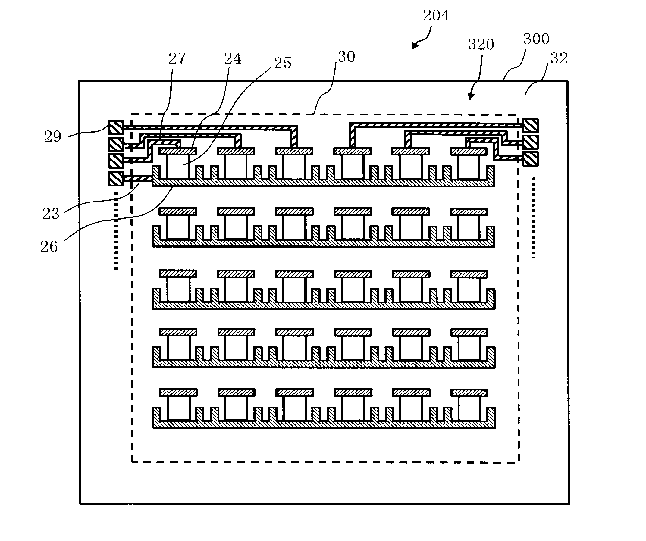
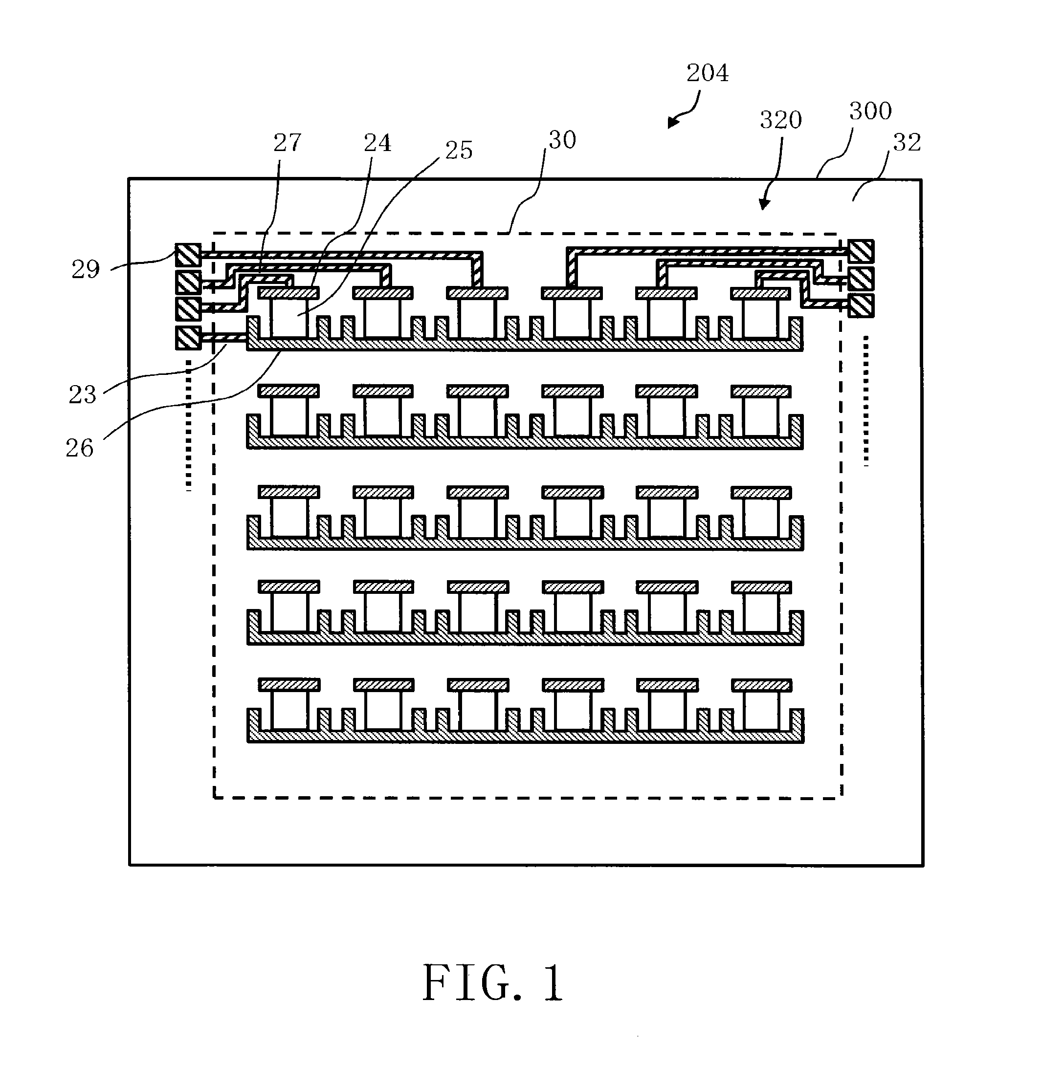
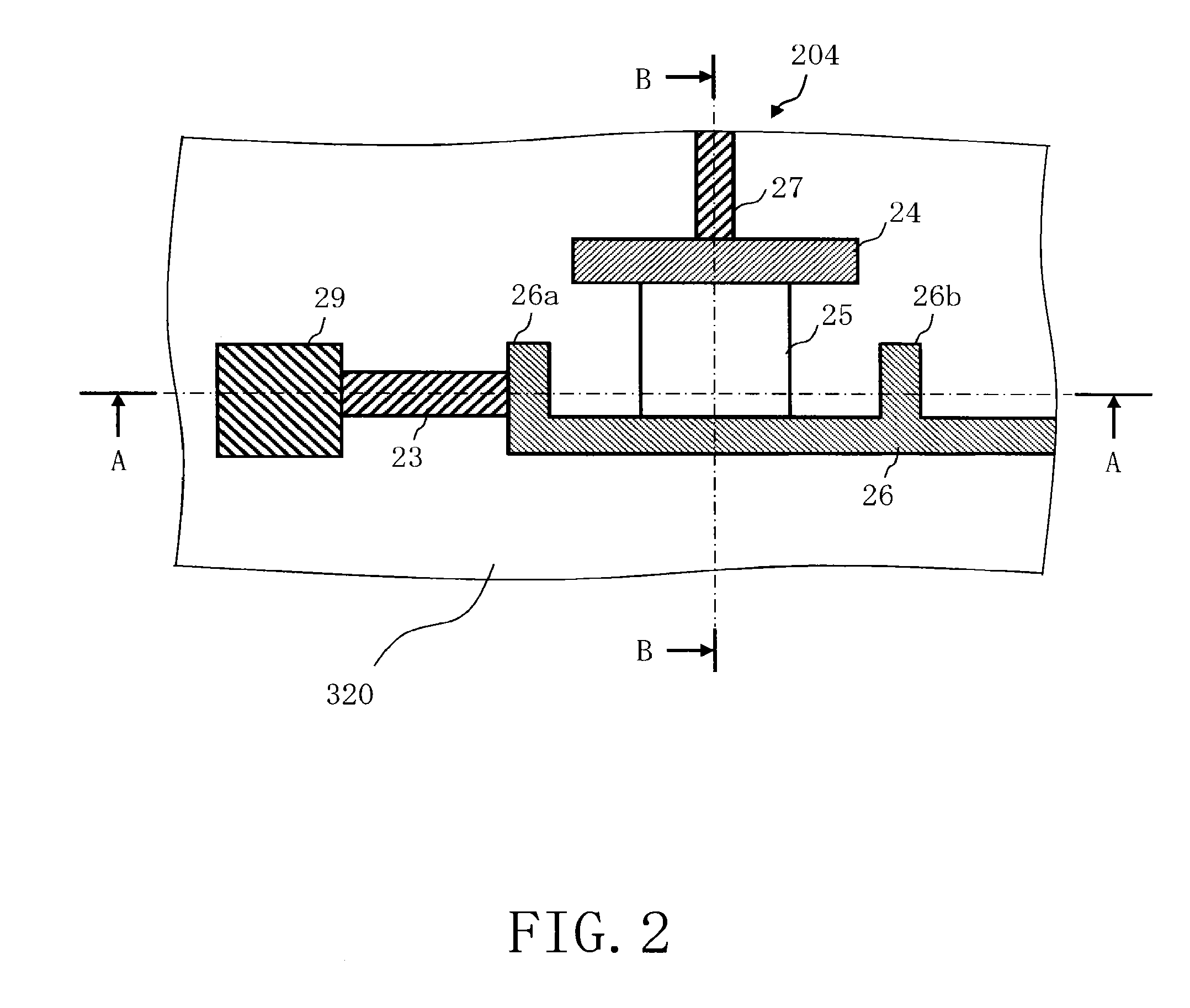
[0019]FIG. 1 is a top view showing a configuration of a blanking aperture array device for multi-beams according to the first embodiment. In FIG. 1, a blanking aperture array device 204 is formed by processing a substrate 300, which is made of silicon (Si), for example, by using semiconductor manufacturing technique. The central part of the substrate 300 is shaved from the back side and processed to be a membrane region 30 having a thin film thickness h. The circumference surrounding the membrane region 30 is a circumference region 32 having a thick film thickness H. The upper surface of the membrane region 30 and the upper surface of the circumference region 32 are formed to be at the same height position, or substantially at the same height position....
PUM
 Abstract
Description
Claims
Application Information