Pillar-shaped semiconductor device and method for producing the same

a semiconductor device and pillar technology, applied in semiconductor devices, basic electric elements, electric devices, etc., can solve the problems of bending and collapse of the si pillar, and achieve the effect of accurate and easy formation

Active Publication Date: 2016-06-02
UNISANTIS ELECTRONICS SINGAPORE PTE LTD
View PDF7 Cites 7 Cited by
  • Summary
  • Abstract
  • Description
  • Claims
  • Application Information

AI Technical Summary

Benefits of technology

[0011]As described above, in the pillar-shaped semiconductor device including SGTs in FIG. 8, there is a demand for a method that allows accurate and easy formation of the N+ region 121b, the P+ r

Problems solved by technology

This tends to result in defects such as b

Method used


Image

  • Pillar-shaped semiconductor device and method for producing the same
  • Pillar-shaped semiconductor device and method for producing the same
  • Pillar-shaped semiconductor device and method for producing the same

Examples


first embodiment

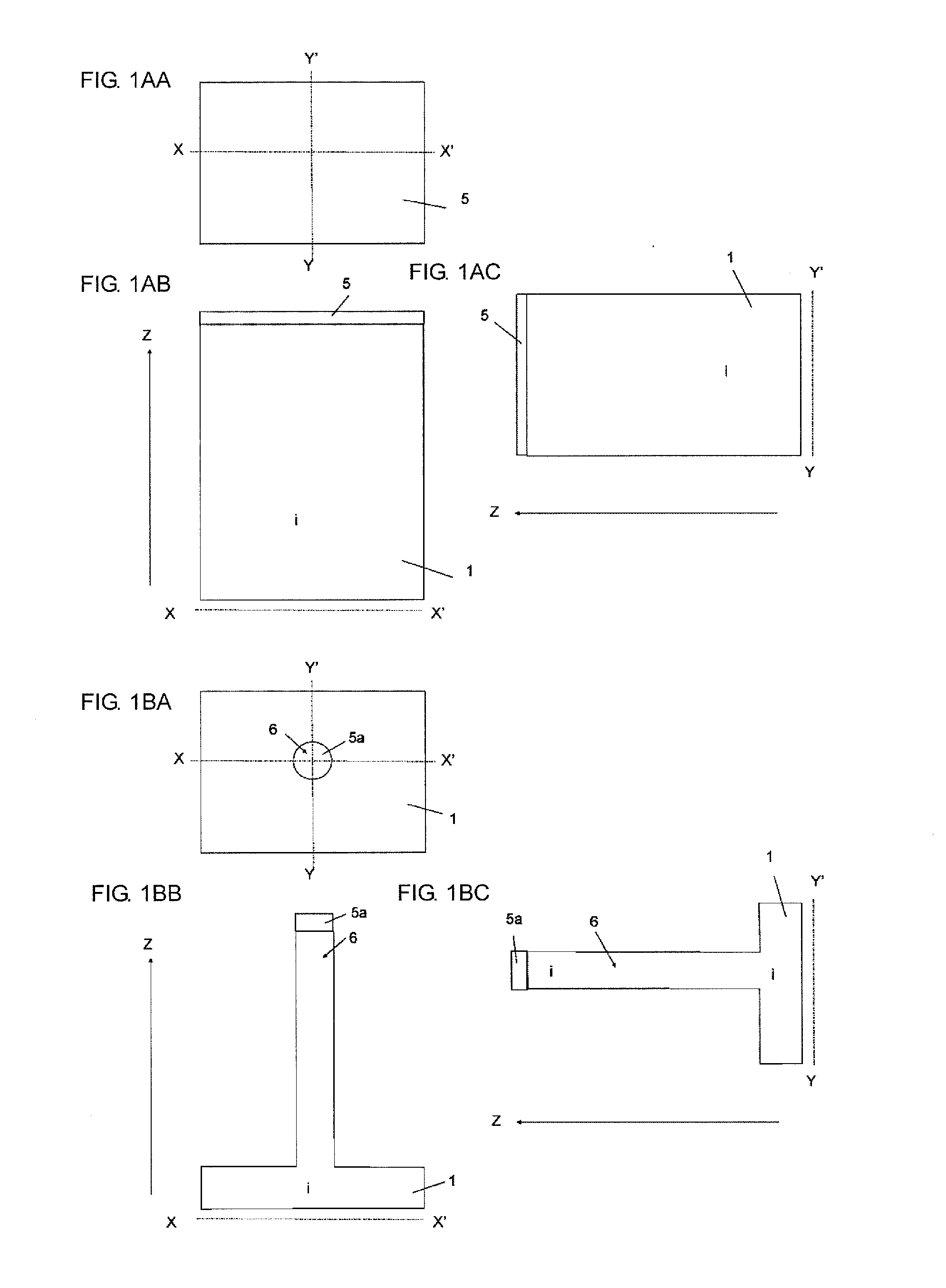
[0054]Hereinafter, a method for producing a CMOS inverter circuit including an SGT according to a first embodiment of the present invention will be described with reference to FIG. 1AA to FIG. 1LC.

[0055]FIGS. 1AA to 1AC are a plan view and sectional views for explanation of a first production step of a CMOS inverter circuit including an SGT: FIG. 1AA is the plan view, FIG. 1AB is a sectional structural view taken along line X-X′ in FIG. 1AA, and FIG. 1AC is a sectional structural view taken along line Y-Y′ in FIG. 1AA. Regarding numbering of these drawings, the same relationship among the suffixes A, B, and C applies to other drawings that will be referred to below.

[0056]As illustrated in FIGS. 1AA to 1AC, a SiO2 layer 5 is formed by thermal oxidation on an i-layer substrate 1.

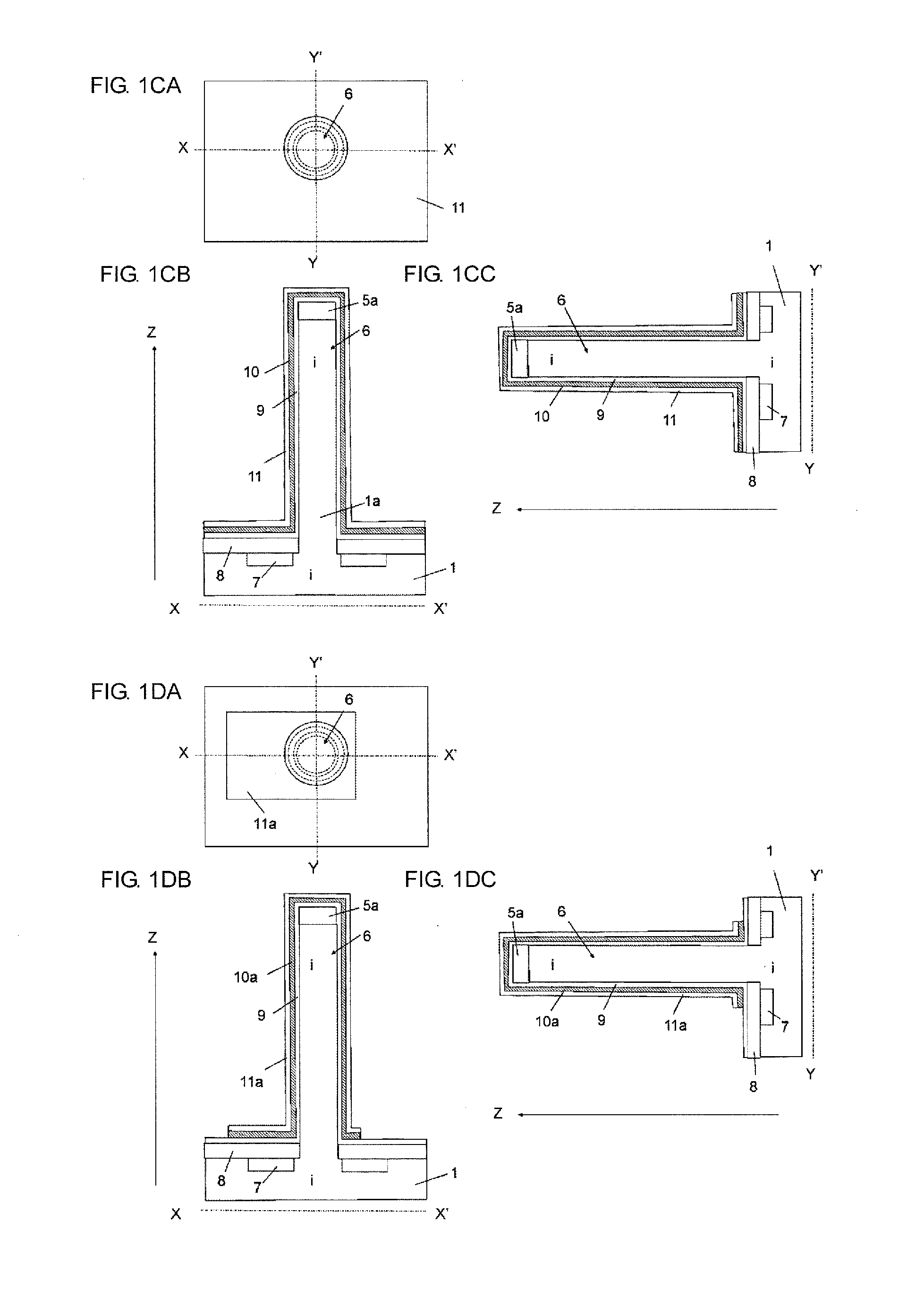
[0057]Subsequently, as illustrated in FIGS. 1BA to 1BC, the SiO2 layer 5 is etched by lithography and RIE (Reactive Ion Etching) to thereby form a SiO2 layer 5a. In addition, RIE using the SiO2 layer 5a as a m...

second embodiment

[0083]Hereinafter, referring to FIG. 2AA to FIG. 2B, a method for producing a CMOS inverter circuit including an SGT according to a second embodiment of the present invention will be described. The CMOS inverter circuit according to the second embodiment is produced by the same steps as those illustrated in FIG. 1AA to FIG. 1LC in the first embodiment except for the following difference in the structure.

[0084]In this embodiment, instead of the NiSi layers 31a and 31b, as illustrated in FIGS. 2AB and 2AC, a NiSi layer 32 connected to the side surfaces of the NiSi layers 20aa and 20bb is formed in the side surface of the Si pillar 6. A contact hole 28e is formed such that the bottom surface thereof is at the surface of the SiO2 layer 17aa. The contact hole 28e is used to mutually connect the output wiring metal layer Vout and the NiSi layer 20bb.

[0085]FIG. 2B is an enlarged view of a dotted rectangle B in FIG. 2AB. The silicide formation from the NiSi layers 20a and 20b into the Si p...

third embodiment

[0087]Hereinafter, referring to FIG. 3AA to FIG. 3BC, a method for producing a CMOS inverter circuit including an SGT according to a third embodiment of the present invention will be described. The CMOS inverter circuit according to the third embodiment is produced by the same steps as those illustrated in FIG. 1AA to FIG. 1LC in the first embodiment except for the following difference in the structure.

[0088]After the same steps as in FIG. 1AA to FIG. 1FC are carried out, as illustrated in FIGS. 3AB and 3AC, heat treatment is carried out to diffuse As atoms in the N+ region 7 into the i-layer substrate to thereby form an N+ region 7a. Subsequently, bias sputtering, for example, is carried out to direct Ni atoms in a direction perpendicular to the upper surface of the i-layer substrate 1, to thereby form a Ni layer 15a on the SiN layer 12a and form a Ni layer 15c on the Si pillar 6. Subsequently, bias sputtering is carried out to form a poly-Si layer 29a not containing impurity atoms...


PUM


Abstract

An opening extending through a gate insulating layer and a gate conductor layer is formed in the circumferential portion of a Si pillar at an intermediate height of the Si pillar. A laminated structure including two sets each including a Ni film, a poly-Si layer containing donor or acceptor impurity atoms, and a SiO2 layer is formed so as to surround the opening. A heat treatment is carried out to form silicide from the poly-Si layers and this silicide formation causes the resultant NiSi layers to protrude and come into contact with the side surface of the Si pillar. The donor or acceptor impurity atoms diffuse from the NiSi layers into the Si pillar to thereby form an N+ region and a P+ region serving as a source or a drain of SGTs.

Description

RELATED APPLICATIONS[0001]The present application claims priority to PCT / JP2014 / 081455, filed Nov. 27, 2014, the entire contents of which are incorporated herein by reference.BACKGROUND OF THE INVENTION[0002]1. Field of the Invention[0003]The present invention relates to a pillar-shaped semiconductor device and a method for producing the pillar-shaped semiconductor device.[0004]2. Description of the Related Art[0005]In recent years, an SGT (Surrounding Gate MOS Transistor), a representative pillar-shaped semiconductor device, has been attracting attention as a semiconductor element providing a semiconductor device having a high integration degree. There has been a demand for a further increase in the integration degrees of semiconductor devices including SGTs.[0006]In a standard planar MOS transistor, the channel extends in a horizontal direction parallel to the upper surface of the semiconductor substrate. In contrast, the channel of an SGT extends in a direction perpendicular to t...

Claims


Application Information

Patent Timeline
IPC IPC(8): H01L29/78H01L29/417H01L29/423H01L29/10H01L21/768H01L21/225H01L21/8234H01L21/24H01L21/265H01L29/66H01L29/08
CPCH01L29/7827H01L29/66666H01L29/41741H01L29/42356H01L29/1037H01L21/768H01L21/225H01L21/823487H01L21/823437H01L21/24H01L21/26513H01L29/0847H01L21/28518H01L21/28531H01L21/31111H01L21/31144H01L21/76805H01L21/823885H01L29/42392
Inventor MASUOKA, FUJIOHARADA, NOZOMU
Owner UNISANTIS ELECTRONICS SINGAPORE PTE LTD
Why Eureka
Try Eureka