Pointer detection sensor and fabrication method for pointer detection sensor
- Summary
- Abstract
- Description
- Claims
- Application Information
AI Technical Summary
Benefits of technology
Problems solved by technology
Method used
Image
Examples
first embodiment
Description of a Fabrication Method for a Pointer Detection Sensor
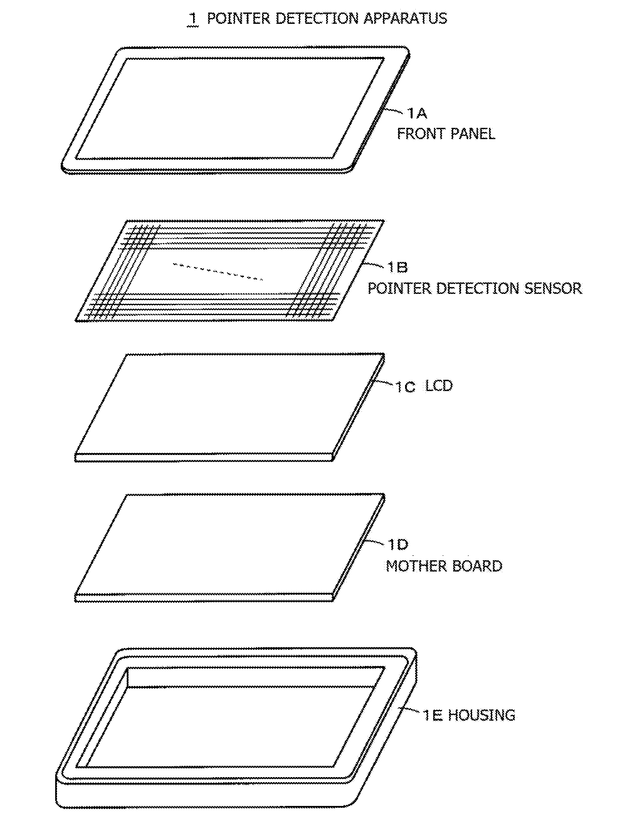
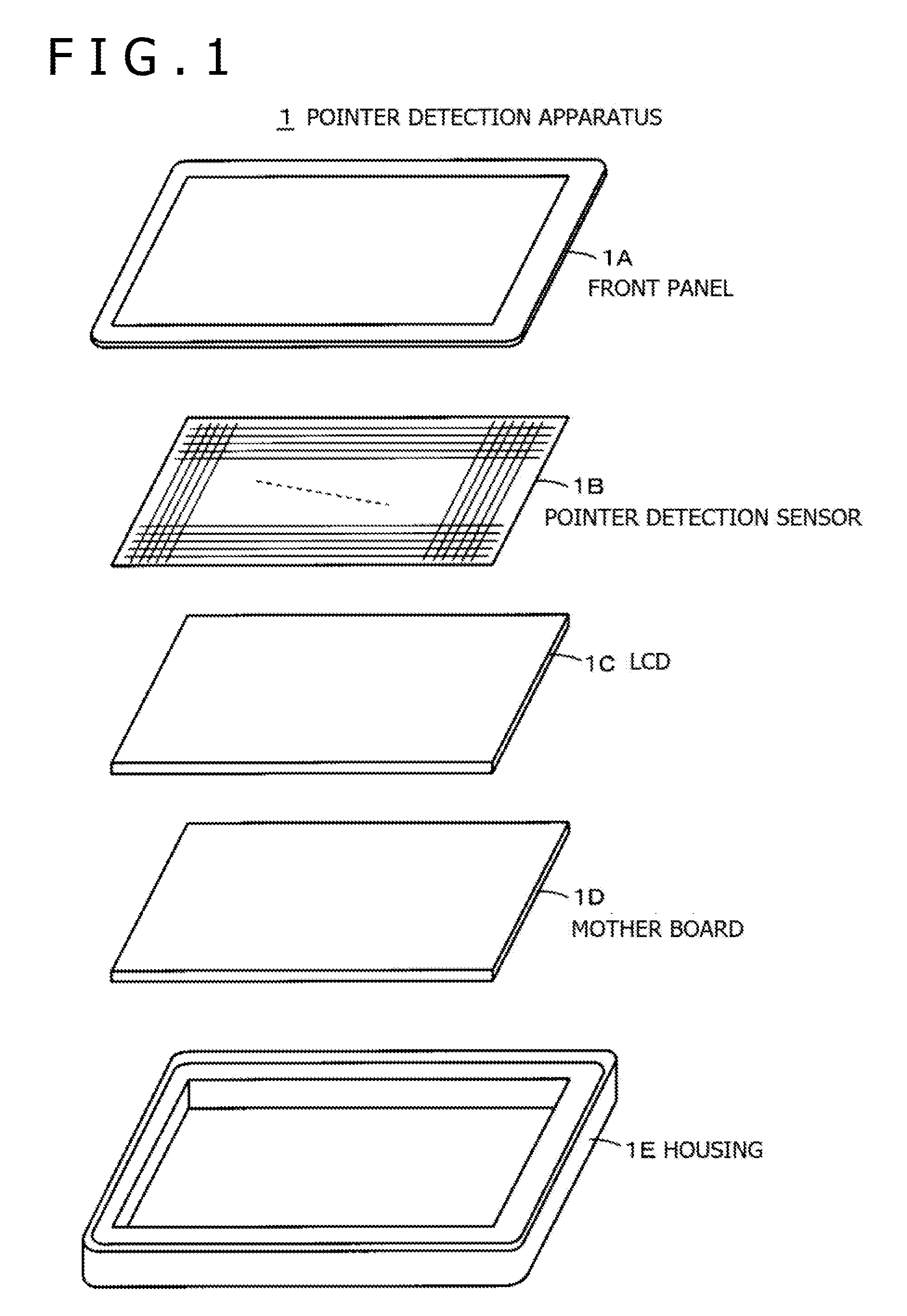
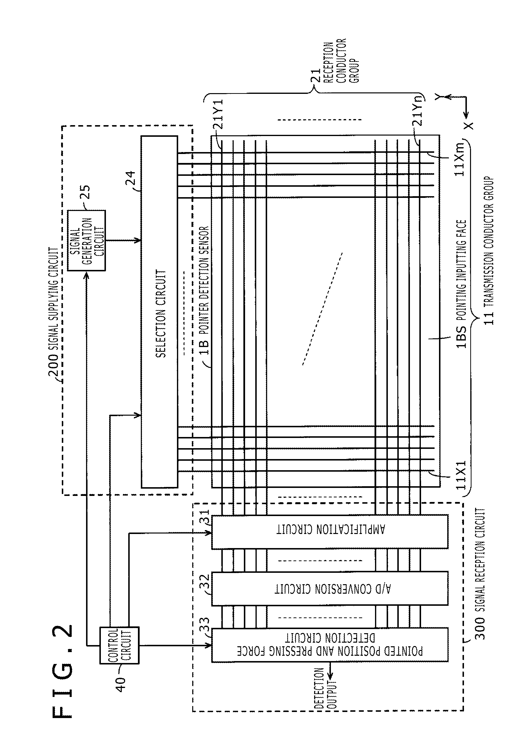
[0179]A first embodiment of the fabrication method for a pointer detection sensor is a method of fabricating the pointer detection sensor 1B described hereinabove. It is to be noted that, while in the pointer detection sensor 1B of the embodiment described above, the spacers Sa to Sd are formed on the second conductors 21Y formed on the lower side substrate 20, in the following description of the first embodiment, it is assumed that spacers are detected as spacers Sa′ to Sd′ on the first electrodes 11X formed on the upper side substrate 10 for the convenience of description.
[0180]First, first conductors 11X are formed on one face side of an upper side substrate 10, and second conductors 21Y are formed on one face side of a lower side substrate 20. Then, the upper side substrate 10 and the lower side substrate 20 are placed such that, in a state in which the first conductors 11X and the second conductors 21Y extend per...
second embodiment
Description of a Fabrication Method
[0189]In the embodiment described above, the spacers are formed such that they extend from the above of ones of the first conductors formed on the upper side substrate 10 and the second conductors formed on the lower side substrate 20 so as to have a determined height spaced from the other ones of the first and second conductors. However, since the OCR comes to have a determined elasticity when it is cured, even if the spacers are formed so as to bridge the first conductors formed on the upper side substrate 10 and the second conductors formed on the lower side substrate 20, it can be expected that characteristics similar to that achieved in the first embodiment described hereinabove can be achieved as characteristics of the distance variation between the first conductors formed on the upper side substrate 10 and the second conductors formed on the lower side substrate 20 caused by pressing by a pointer.
[0190]The second embodiment is an example whe...
PUM
| Property | Measurement | Unit |
|---|---|---|
| Shape | aaaaa | aaaaa |
| Height | aaaaa | aaaaa |
| Transparency | aaaaa | aaaaa |
Abstract
Description
Claims
Application Information


