Electric-programmable magnetic module and picking-up and placement process for electronic devices

a technology of electronic devices and magnetic modules, which is applied in the direction of magnetic bodies, semiconductor/solid-state device testing/measurement, instruments, etc., can solve the problems of difficult to achieve the growth of light emitting layers on the same substrate, low conversion efficiency of wavelength conversion materials, and difficult to uniformly coat wavelength conversion materials

Active Publication Date: 2016-06-16
PLAYNITRIDE +1
View PDF5 Cites 32 Cited by
  • Summary
  • Abstract
  • Description
  • Claims
  • Application Information

AI Technical Summary

Problems solved by technology

Since lattice constants of the light emitting layers capable of emitting different colored lights are different, growth of the light emitting layers on a same substrate is difficult to be achieved.
However, the conversion efficiency of the wavelength conversion materials is low and it is difficult to coat the wavelength conversion materials uniformly.
To one ordinary skilled in the art, how to efficiently pick-up and place the LED chips to a circuit substrate of the monolithic micro-display is an important issue.

Method used


Image

  • Electric-programmable magnetic module and picking-up and placement process for electronic devices
  • Electric-programmable magnetic module and picking-up and placement process for electronic devices
  • Electric-programmable magnetic module and picking-up and placement process for electronic devices

Examples


first embodiment

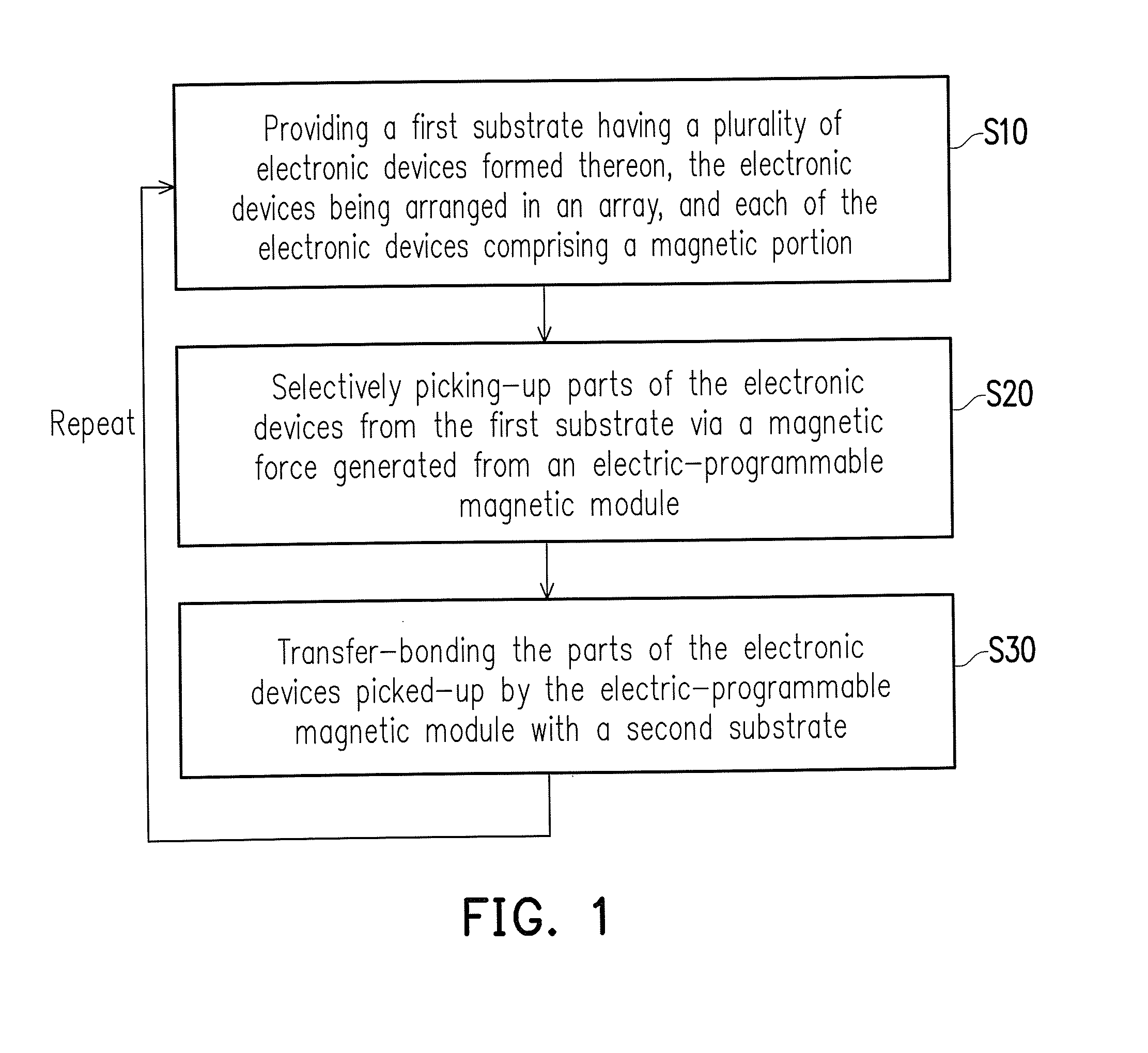
[0022]FIG. 1 is a flowchart schematically illustrates a picking-up and placement process for electronic devices in accordance with this disclosure. Referring to FIG. 1, the picking-up and placement process for electronic devices comprises the following steps (S10, S20 and S30). First of all, a first substrate having a plurality of electronic devices formed thereon is provided, wherein the electronic devices are arranged in an array and each of the electronic devices comprises a magnetic portion formed thereon or embedded therein (Step S10). After the first substrate is provided, parts of the electronic devices are selectively picked-up from the first substrate via a magnetic force generated from an electric-programmable magnetic module (Step S20). Then, the parts of the electronic devices picked-up by the electric-programmable magnetic module are bonded with a second substrate (Step S30). In one of exemplary embodiments of this disclosure, the picking-up and placement process for el...

second embodiment

[0046]FIG. 5 is a block diagram of a control system for the electric-programmable magnetic module shown in FIG. 3. Referring to FIG. 5, the control system 300 of this embodiment includes a computer 310, an electrical control unit 320, a mechanical control unit 330 and a heating control unit 340, wherein the electrical control unit 320, the mechanical control unit 330 and the heating control unit 340 are electrically connected to the computer 310. For example, the computer 310 and the electrical control unit 320 control operation of the MEMS chip 210 (e.g. selectively pick-up, in-situ testing). The computer 310 and the mechanical control unit 330 control movement of the bonding equipment 220 (shown in FIG. 3). The computer 310 and the heating control unit 340 control parameters of the heating process during the picking-up and placement process.

third embodiment

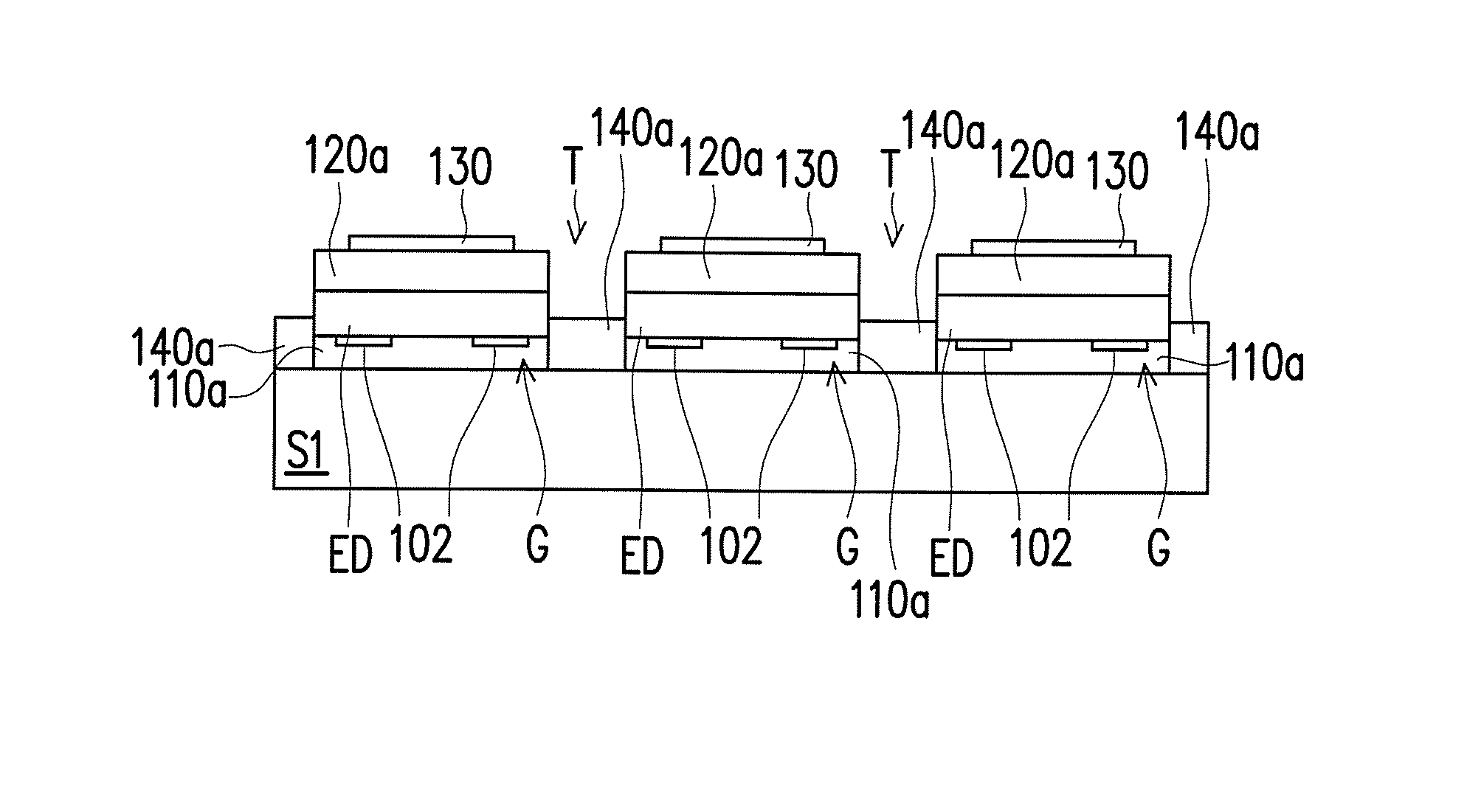
[0047]FIG. 6A through FIG. 6K are cross-sectional views of a picking-up and placement process for electronic devices in accordance with the third embodiment of the disclosure.

[0048]Referring to FIG. 6A through FIG. 6K, the picking-up and placement process for electronic devices in accordance with this embodiment is similar with the picking-up and placement process of the first embodiment except that the sacrificial layer 120 disclosed in the first embodiment is omitted in this embodiment. Specifically, after the photoelectric semiconductor layer 100 is bonded with the first substrate S1 through the adhesive 110, since the electrodes 102 are magnetic electrodes, no sacrificial layer (120) and magnetic portions (130) are required to be formed on the surface 100a of the photoelectric semiconductor layer 100 and the photoelectric semiconductor layer 100 and the adhesive 110 are patterned to form the electronic devices ED and a plurality of adhesive patterns 110a disposed under the elect...


PUM


Abstract

A picking-up and placement process for electronic devices comprising: (a) providing a first substrate having a plurality of electronic devices formed thereon, the electronic devices being arranged in an array, and each of the electronic devices comprising a magnetic portion; (b) selectively picking-up parts of the electronic devices from the first substrate via a magnetic force generated from an electric-programmable magnetic module; and (c) bonding the parts of the electronic devices picked-up by the electric-programmable magnetic module with a second substrate.

Description

CROSS-REFERENCE TO RELATED APPLICATION[0001]This application claims the priority benefits of U.S. provisional application Ser. No.62 / 085,657, filed on Dec. 1, 2014, and Taiwan application serial no. 103143505, filed on Dec. 12, 2014. The entirety of each of the above-mentioned patent applications is hereby incorporated by reference herein and made a part of this specification.[0002]BACKGROUND OF THE DISCLOSURE[0003]1. Technical Field[0004]The present disclosure generally relates to a picking-up and placement process for electronic devices, in particular, to a picking-up and placement process for electronic devices using an electric-programmable magnetic module.[0005]2. Description of Related Art[0006]Inorganic light emitting diodes (LEDs) have features of self-luminous, high brightness and so on, and therefore have been widely applied in the fields of illumination, display, projector and so forth. Taking monolithic full color micro-LED displays as an example, monolithic micro-displa...

Claims


Application Information

Patent Timeline
Patent Type & Authority Applications(United States)
IPC IPC(8): H01L21/66H01L33/48H01L21/683H01L33/00
CPCH01L22/20H01L33/0095H01L2933/0033H01L21/683H01L33/48H01L24/75H01L24/81G01R31/2635H01L2224/75H01L2221/68327H01L2221/68354H01L2221/68381H01L21/67144H01L21/6835H01L2221/6835H01L22/22H01L33/06H01L33/12H01L33/62H01L2221/68368H01L2933/0066
Inventor WU, MING-HSIENFANG, YEN-HSIANGCHAO, CHIA-HSIN
Owner PLAYNITRIDE
Why Eureka
Try Eureka