Display device using semiconductor light emitting device

Active Publication Date: 2016-06-30
LG ELECTRONICS INC
View PDF10 Cites 38 Cited by
  • Summary
  • Abstract
  • Description
  • Claims
  • Application Information

AI Technical Summary

Benefits of technology

[0015]According to the present disclosure having the foregoing configuration, a distance between light emitting devices may be sufficiently large and the conductive adhesive layer may have softness, thereby implementing a rollable display device.
[0016]According to an embodiment, an inorganic semiconductor light emitting device may be disposed in a pixel region, thereby having an advantage capable of implementing a high-speed screen with a fast response time.
[0017]Furthermore, according to an embodiment, an additional back light may be not required, thereby having an adv

Problems solved by technology

However, there exist problems such as not-so-fast response time, difficult implementation of flexibility in case of LC

Method used


Image

  • Display device using semiconductor light emitting device
  • Display device using semiconductor light emitting device
  • Display device using semiconductor light emitting device

Examples


Embodiment Construction

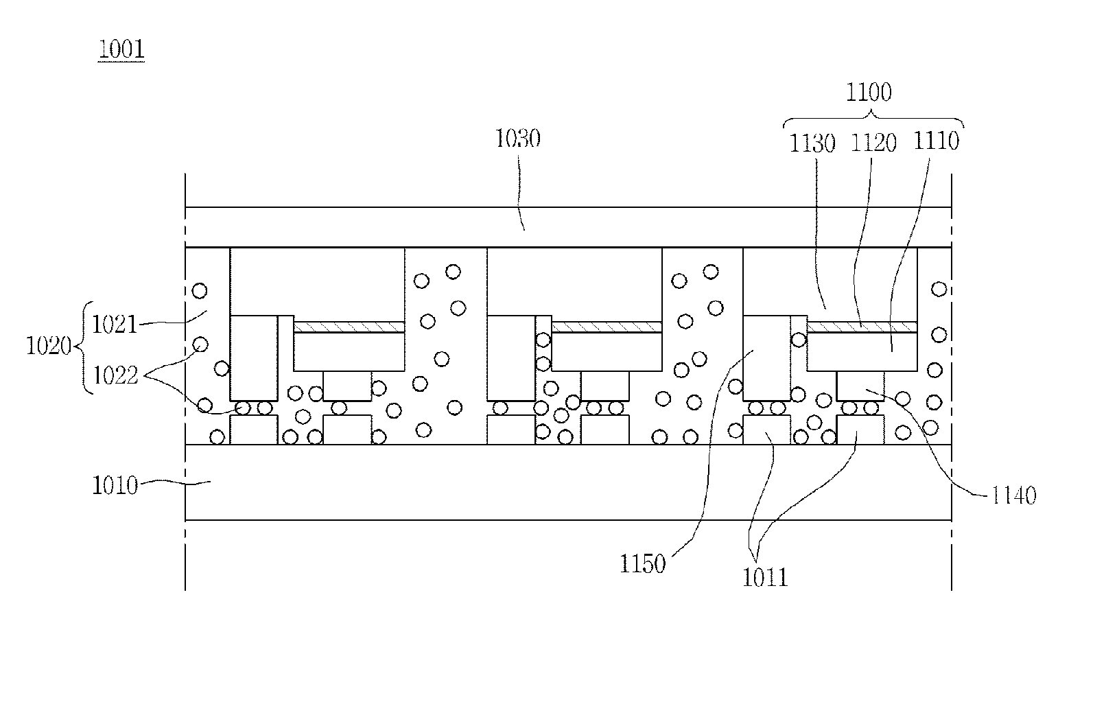
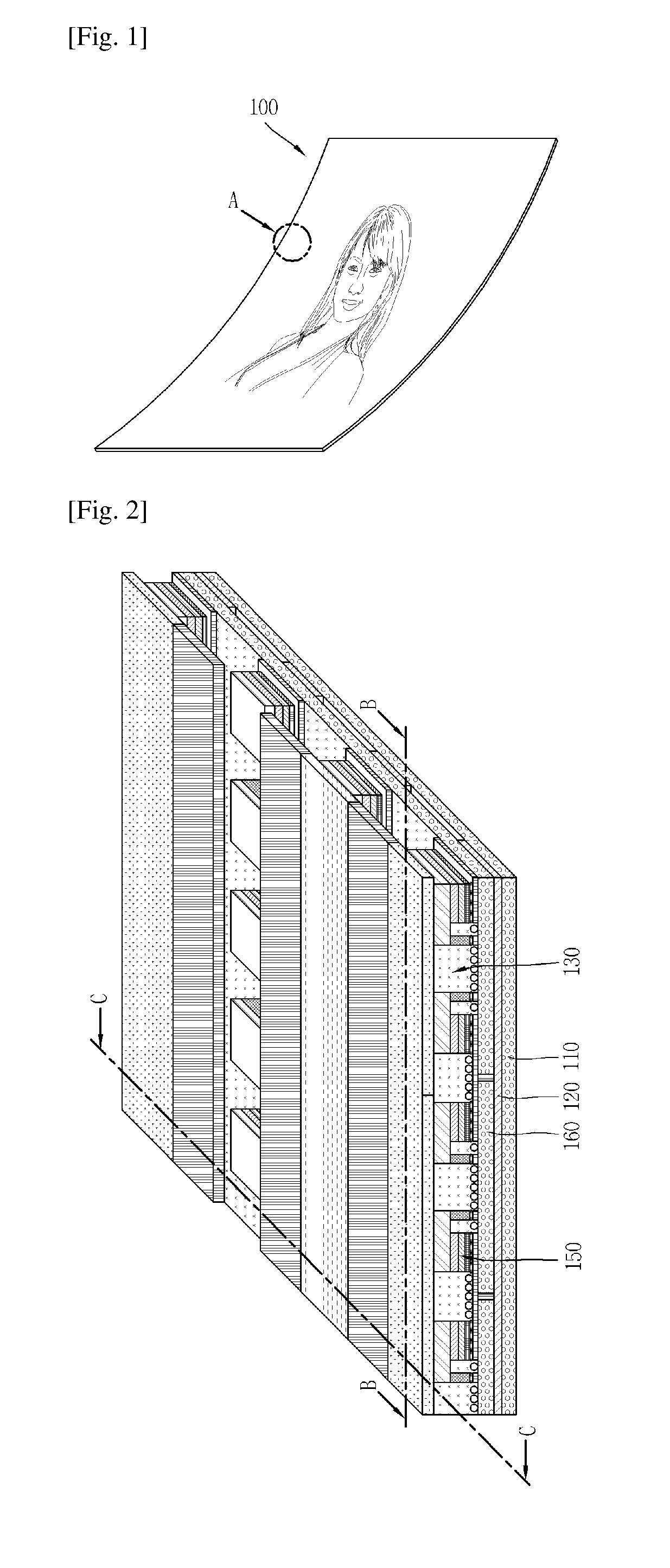
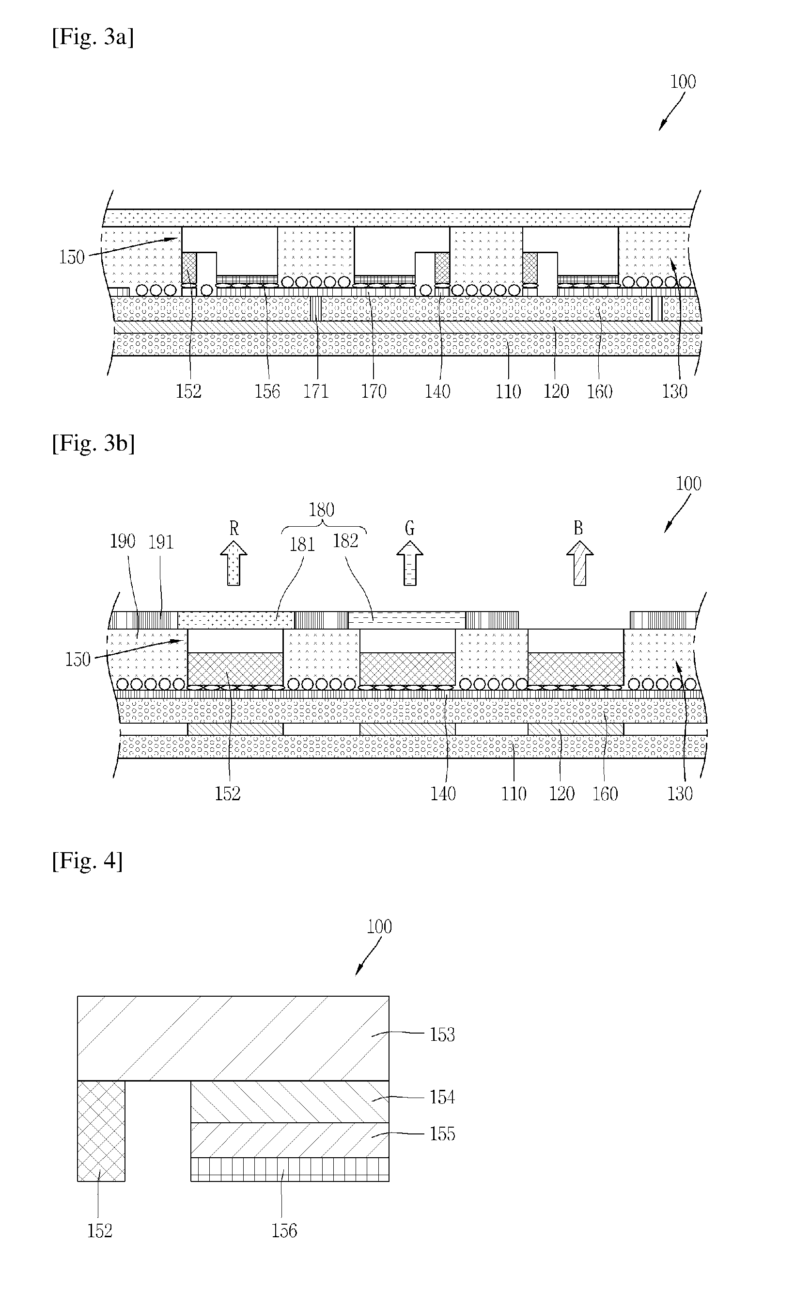
[0034]Advantages and features of the present disclosure, and methods of accomplishing the same will be clearly understood with reference to the following embodiments described in detail in conjunction with the accompanying drawings. However, the present disclosure is not limited to those embodiments disclosed below but may be implemented in various different forms. It should be noted that the present embodiments are merely provided to make a full disclosure of the invention and also to allow those skilled in the art to know the full range of the invention, and therefore, the present invention is to be defined only by the scope of the appended claims. Further, like reference numerals refer to like or similar elements throughout the specification.

[0035]Spatially relative terms such as “below”, “beneath”, “lower”, “above”, or “upper” may be used herein to describe a correlation between one device or constituent element and other devices or constituent elements as illustrated in the dra...


PUM


Abstract

A display device according to an embodiment of the present disclosure may include a lower substrate disposed with a line electrode at an upper portion thereof, a plurality of semiconductor light emitting devices electrically connected to the line electrode to generate light, a wavelength converter disposed on the semiconductor light emitting device to convert a wavelength of light generated from the semiconductor light emitting device, and a conductive adhesive layer comprising conductors configured to electrically connect the lower substrate to the semiconductor light emitting device and a body configured to surround the conductors, wherein the semiconductor light emitting device has a composition formula of InxAlyGa1-x-yN (0≦x≦1, 0≦y≦1, 0≦x+y≦1).

Description

TECHNICAL FIELD[0001]The present disclosure relates to a display device, and more particularly, to a display device using a semiconductor light emitting device.BACKGROUND ART[0002]In recent years, display devices having excellent characteristics such as low profile, flexibility and the like have been developed in the display technical field. On the contrary, currently commercialized main displays are represented by liquid crystal displays (LCDs) and active matrix organic light emitting diodes (AMOLEDs).[0003]However, there exist problems such as not-so-fast response time, difficult implementation of flexibility in case of LCDs, and there exist drawbacks such as short life span, not-so-good yield as well as low flexibility in case of AMOLEDs.[0004]On the other hand, light emitting diodes (LEDs) are well known light emitting devices for converting an electrical current to light, and have been used as a light source for displaying an image in an electronic device including information ...

Claims


Application Information

Patent Timeline
IPC IPC(8): H01L25/075H01L33/46H01L33/50H01L33/32H01L33/62
CPCH01L25/0753H01L33/32H01L33/46H01L33/50H01L33/62H01L2224/16H01L2924/0002H05B33/145H05B33/24H05B33/26G09F9/00H05B33/02C09K11/62C09K11/64C09K11/0883H01L2924/00
Inventor RHEE, BYUNGJOONCHOI, YOONHO
Owner LG ELECTRONICS INC
Why Eureka
Try Eureka