Printed wiring board and connector connecting the wiring board

a technology of printed wiring board and connector, which is applied in the direction of printed circuit details, printed circuit aspects, coupling device connections, etc., can solve the problems of weak holding force given by the connector to the connection end portion, contact failure, etc., and achieve the effect of reducing the degree of freedom of wiring in the wiring board, enhancing the disconnection resistance of printed wiring board, and enhancing the strength

Active Publication Date: 2016-07-14
THE FUJIKURA CABLE WORKS LTD +1
View PDF8 Cites 4 Cited by
  • Summary
  • Abstract
  • Description
  • Claims
  • Application Information

AI Technical Summary

Benefits of technology

[0019]The engageable part formed at the printed wiring board may not be enough only with the strength of the base substrate because the engageable part is pulled by a metal engagement part of another electronic component (e.g., a tab-like lock member of a connector to be described later). Accordingly, the present inventors have proposed to provide a reinforcement layer at the frontward side with respect to the engageable part in order to enhance the strength, and further to form such a reinforcement layer integrally with a pad for electrical connection that is located at the outermost side in the width direction of the connection end portion, in order to respond to requests of space saving and the like. When designing a wiring board, however, there are many situations that the above described engagement part of an electronic component, which is not used for signal transmission, is practically connected to ground, and if the engagement part is erroneously connected with the reinforcement layer, the pad for signal at the outermost side in the width direction of the printed wiring board will short-circuit with ground, leading to a risk that the signal leaks. Such signal leaking may be avoided if the engagement part is not connected to ground. However, if the engagement part is not connected to ground, the degree of freedom of wiring in the wiring board will be reduced.
[0020]In view of the above, the first aspect of the present invention has a feature that the insulating layer is provided on the surface of the reinforcement layer which is formed integrally with at least any one of the pads and wirings. According to this feature, the disconnection resistance of the printed wiring board can be enhanced while the signal in the pad can be prevented from transmitting via the reinforcement layer to the engagement part of another electronic component, which may be connected to ground. The above described problem of short-circuiting to ground can thus be solved. The second aspect of the present invention has a feature that the reinforcement layer is formed separately from the pads and wirings. According to this feature, the disconnection resistance of the printed wiring board can be enhanced while the signal in the pad can be prevented from transmitting via the reinforcement layer to the engagement part of another electronic component, which may be connected to ground. The above described problem of short-circuiting to ground can thus be solved.
[0021]Therefore, according to the present invention, a printed wiring board having excellent disconnection resistance can be provided, and the problem of short-circuiting to ground due to the reinforcement layer can also be solved.

Problems solved by technology

However, if a printed wiring board is made thin and small, the holding force given by a connector to the connection end portion will be weak, and troubles may possibly occur, including that the printed wiring board is disconnected from the connector and contact failure occurs during implementation such as due to reaction forces in wiring and impact of dropping or the like.

Method used


Image

  • Printed wiring board and connector connecting the wiring board
  • Printed wiring board and connector connecting the wiring board
  • Printed wiring board and connector connecting the wiring board

Examples


example 1

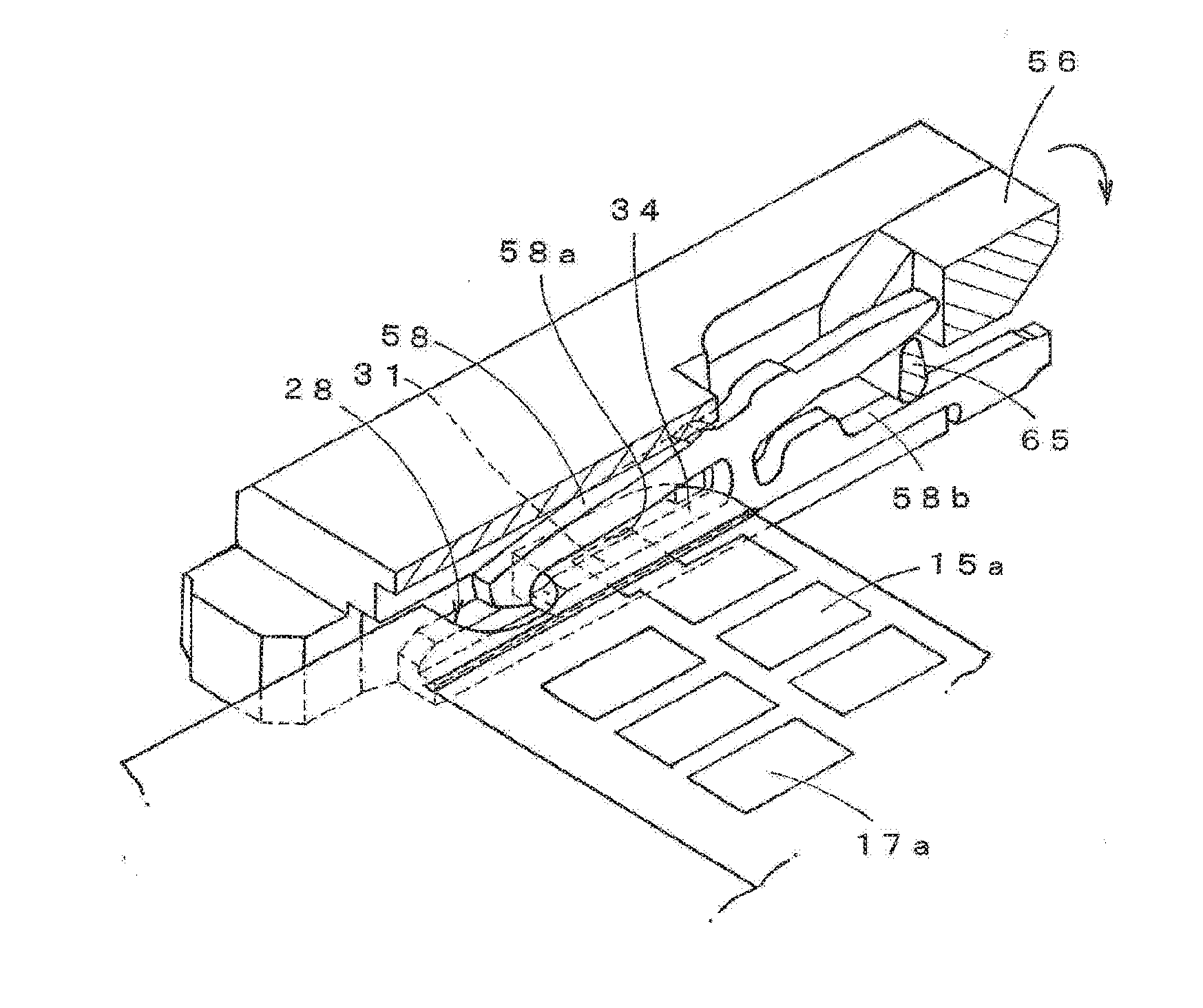
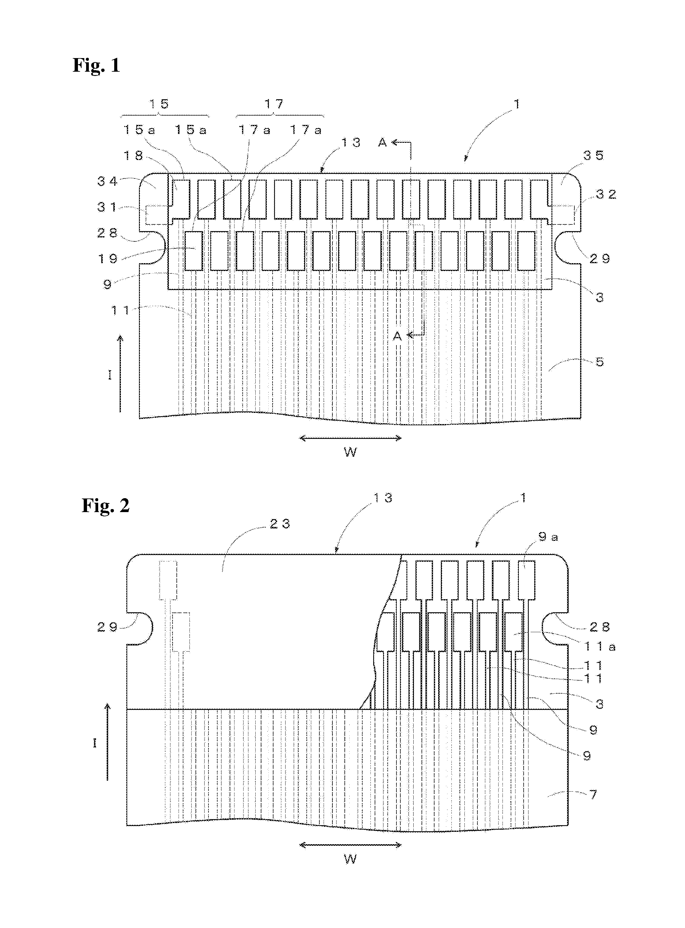
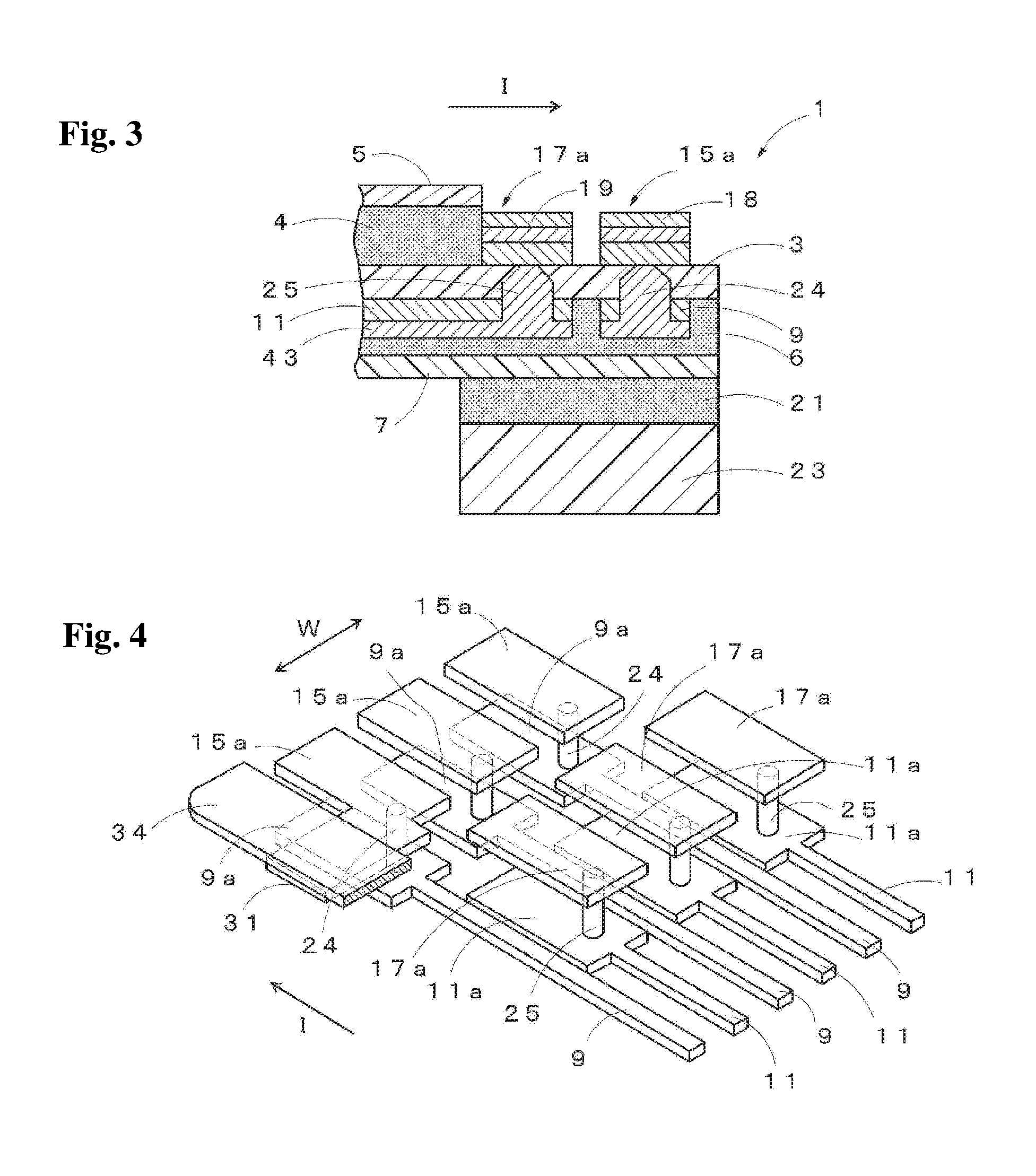
[0092]As Example 1, a printed wiring board having the structure shown in FIGS. 1 to 4 was experimentally manufactured. Specifically, the flexible printed wiring board was manufactured such that: the connection end portion had pads disposed in a staggered arrangement to form 15 pads of the front array and 14 pads of the rear array; the pitch of the pads was 0.175 mm (0.35 mm in each array); both the wirings for the pads of the front array and the wirings for the pads of the rear array were provided on the surface (back surface) of the base film opposite to the surface provided with the pads; and reinforcement layers formed integrally with the pads were provided at the top surface side and at the frontward side with respect to notched parts (engageable parts). In addition, insulating layers were formed on the upper surfaces of the reinforcement layers using extended parts of an upper surface side coverlay. The pads, wirings and reinforcement layers were made of copper, and gold plated...

example 2

[0093]As Example 2, a printed wiring board was experimentally manufactured as in Example 1 except that the reinforcement layers at the top surface side (the side provided with the pads) of the base film were formed separately from the pads as shown in FIG. 13 and insulating layers covering the reinforcement layers were not provided.

example 3

[0094]As Example 3, a printed wiring board was experimentally manufactured as in Example 2 except that insulating layers covering the reinforcement layers were provided as shown in FIG. 14. In more detail, the flexible printed wiring board of Example 3 was manufactured such that the insulating layers covering the reinforcement layers were constituted of extended parts extending frontward from the outer side parts of the upper surface side coverlay in the width direction.


PUM


Abstract

A printed wiring board (1) includes: a base substrate (3); a plurality of pads (15a, 17a) for electrical connection that are disposed at one surface side of the base substrate (3) and at a connection end portion (13) to be connected with another electronic component (50); wirings (9, 11) that are connected with the pads (15a, 17a); and engageable parts (28, 29) that are formed at side edge parts of the connection end portion (13) and are to be engaged with engagement parts (58) of the other electronic component (50) in the direction of disconnection. The flexible printed wiring board (1) further includes: reinforcement layers (31, 32) that are disposed at the one surface side of the base substrate (3) and at a frontward side with respect to the engageable parts (28, 29) when viewed in the direction of connection with the other electronic component and that are formed integrally with the pads (15a); and insulating layers (34, 35) that cover the reinforcement layers (31, 32).

Description

TECHNICAL FIELD[0001]The present invention relates to a printed wiring board having pads for electrical connection at a connection end portion to be connected with another electronic component, such as a connector, and also relates to a connector that connects the printed wiring board with another wiring board.BACKGROUND ART[0002]Printed wiring boards are used for connection between electronic components in electronic devices, such as digital cameras, digital video camcorders, notebook-sized personal computers, cellular phones, and game machines. In accordance with reduction in weight, thickness and size of such electronic devices, it is also required to make printed wiring boards thin and small in themselves. However, if a printed wiring board is made thin and small, the holding force given by a connector to the connection end portion will be weak, and troubles may possibly occur, including that the printed wiring board is disconnected from the connector and contact failure occurs ...

Claims


Application Information

Patent Timeline
Patent Type & Authority Applications(United States)
IPC IPC(8): H01R12/73H05K1/11
CPCH01R12/73H05K2201/10189H05K1/111H01R12/77H01R12/88H05K1/117H05K2201/09036H05K2201/09063H05K2201/09409
Inventor ISHIDA, YUKISUZUKI, MASAYUKINAKANO, YUKIURAI, HARUNORINAGAE, NORIFUMI
Owner THE FUJIKURA CABLE WORKS LTD
Why Eureka
Try Eureka