Semiconductor device

a technology of semiconductors and devices, applied in the field of semiconductor devices, can solve problems such as errors, and achieve the effect of improving operational reliability and accuracy

Active Publication Date: 2016-07-28
SK HYNIX INC
View PDF2 Cites 8 Cited by
  • Summary
  • Abstract
  • Description
  • Claims
  • Application Information

AI Technical Summary

Benefits of technology

[0006]An embodiment is directed to a semiconductor device capable of improving operational reliability and accuracy.

Problems solved by technology

However, an error may occur due to the threshold voltage of the memory cell being sensed incorrectly when a read operation is performed after the program loop or the erase loop is performed.

Method used


Image

  • Semiconductor device
  • Semiconductor device
  • Semiconductor device

Examples


Embodiment Construction

[0016]Hereinafter, various exemplary embodiments will be described in detail with reference to the accompanying drawings. In the drawings, thicknesses and lengths of components may be exaggerated for convenience of Illustration. In the following description, a detailed explanation of related functions and constitutions may be omitted for simplicity and conciseness of explanation. Like reference numerals refer to like elements throughout the specification and drawings.

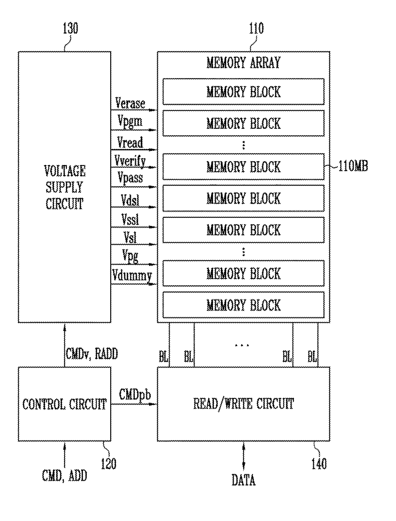
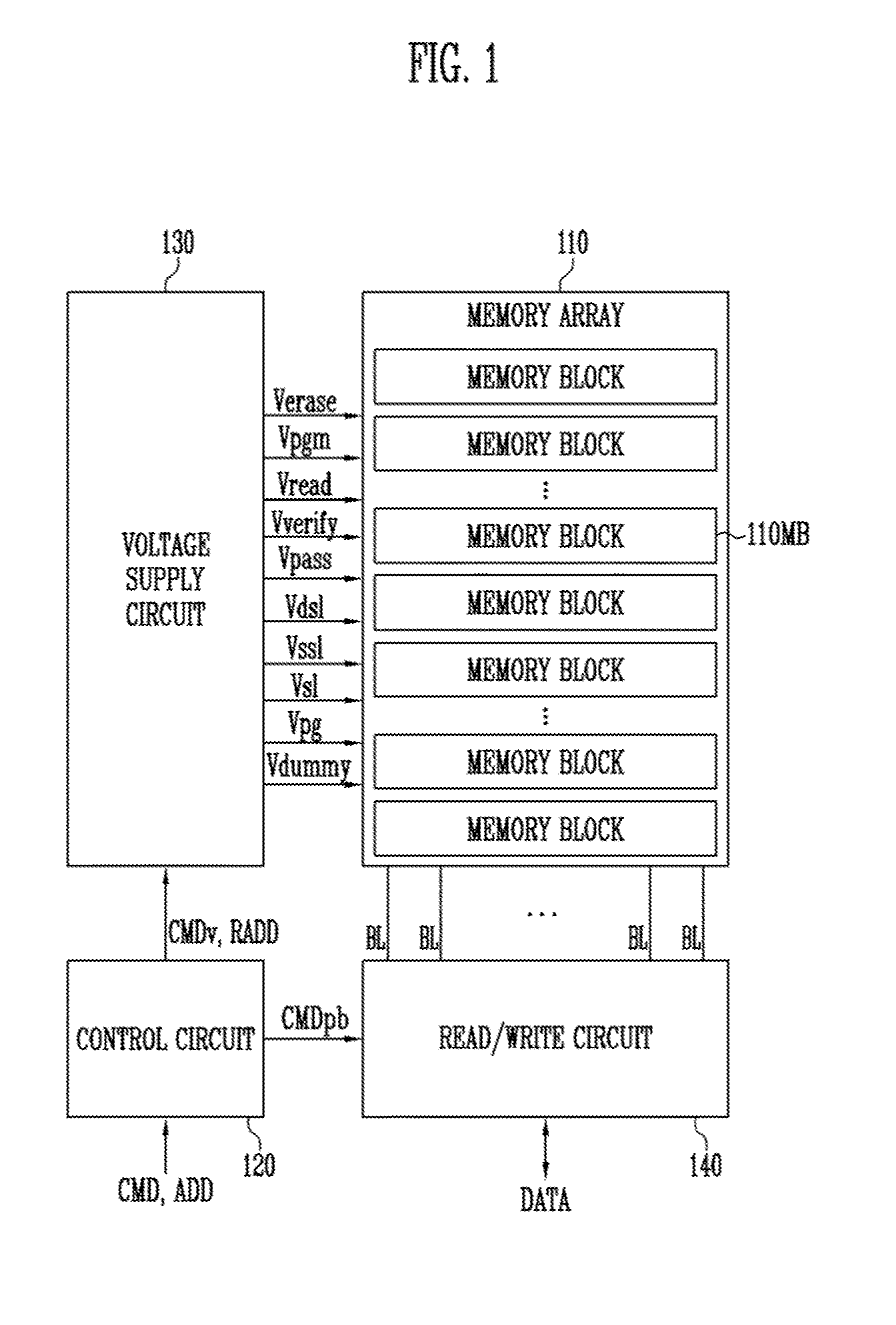
[0017]FIG. 1 is a block diagram illustrating a semiconductor device according to an embodiment.

[0018]Referring to FIG. 1, the semiconductor device may include a memory array 110 and an operation circuit 120 to 140. The memory array 110 may include a plurality of memory blocks 110MB. Each of the memory blocks 110MB may include a plurality of memory strings. Each of the memory strings may include a plurality of memory cells (not illustrated). In a flash memory device, each memory block may include flash memory cells. Each...


PUM


Abstract

A semiconductor device includes a plurality of memory blocks including a plurality of memory cells, wherein the plurality of memory cells are divided into a plurality of pages; and an operation circuit configured to output operating voltages to local lines of a selected memory block, among the plurality of memory blocks, to perform a program operation, a read operation and an erase operation on the selected memory block, wherein the operation circuit is configured to apply a dummy pulse having a positive potential to the local lines of the selected memory block after completing the program operation, the read operation and the erase operation

Description

CROSS-REFERENCE TO RELATED APPLICATION[0001]The present application is a Continuation in Part of U.S. patent application Ser. No. 14 / 686,492 filed on Apr. 14, 2015 which claims priority to Korean patent application number 10-2014-0160704, filed on Nov. 18, 2014, the entire disclosure of which is herein incorporated in its entirety.BACKGROUND[0002]1. Field of Invention[0003]Various exemplary embodiments relate generally to a semiconductor device and, more particularly, to a semiconductor device including a memory cell.[0004]2. Description of Related Art[0005]A program loop may be performed to store data in a memory cell. A read operation may be performed to read data stored in the memory cell. An erase loop may be performed to erase the data stored in the memory cell. The threshold voltage of the memory cell may be sensed to read the data stored in the memory cell. However, an error may occur due to the threshold voltage of the memory cell being sensed incorrectly when a read operati...

Claims


Application Information

Patent Timeline
Patent Type & Authority Applications(United States)
IPC IPC(8): G11C16/14G11C16/28
CPCG11C16/28G11C16/14G11C7/1048G11C8/12G11C16/0483G11C16/08G11C16/10G11C16/16G11C16/26G11C16/30
Inventor AN, CHI WOOK
Owner SK HYNIX INC
Why Eureka
Try Eureka