Semiconductor device and method of manufacturing the same

a semiconductor device and semiconductor technology, applied in the direction of semiconductor devices, electrical equipment, transistors, etc., can solve the problems of rcat frequently failing, unable to obtain a sufficient refresh time of memory devices, and insufficient electrical insulation between drain regions, so as to improve the operational reliability and stability of semiconductor devices. , the effect of high integration degr

Active Publication Date: 2016-07-07
SAMSUNG ELECTRONICS CO LTD
View PDF2 Cites 19 Cited by
  • Summary
  • Abstract
  • Description
  • Claims
  • Application Information

AI Technical Summary

Benefits of technology

[0054]Thus, although the storage node contact may expand over the alignment marginal area of the field region around the source junction due to the misalignment of the source junction and the storage node contact hole, the electrical shortage between the neighboring bit line contact and the storage node contact may be sufficiently prevented by the junction separator. Since the junction separator may have much more etch-resistive than the device isolation layer such as the sidewall oxide layer, the high insulating materials may be still remain in the neighborhood of the source junction including the alignment marginal area and thus the source junction may be sufficiently isolated by the junction separator in spite of the cell size reduction. The drain junction D may also be defined and insulated by the same junction separator in the same way. Therefore, the electrical connection between the neighboring source and drain junctions may be prevented by the junction separator when the semiconductor devices are downsized with high integration degree, thereby improving the operational reliability and stability of the semiconductor devices.

Problems solved by technology

Thus, it has been getting more difficult to obtain a sufficient refresh time of memory devices due to the short channel effect.
However, the RCAT frequently fails by a high gate-induced drain leakage (GIDL).
Particularly, the isolation layer defining the drain region is likely to be removed from the substrate in an etching process for forming the contact hole in the drain region, thus the electrical insulation tends to be insufficient between the drain region and a neighboring source region.
The insufficient electrical insulation between the drain region and the source region leads to the electrical short between the bit line contact and the storage node contact.
In addition, the gap distance between the neighboring source and drain regions may also be reduced due to the reduction of the occupation area, which makes it difficult to obtain a sufficient aligning margin when forming the bit line contact hole and the storage node contact hole.

Method used


Image

  • Semiconductor device and method of manufacturing the same
  • Semiconductor device and method of manufacturing the same
  • Semiconductor device and method of manufacturing the same

Examples


Embodiment Construction

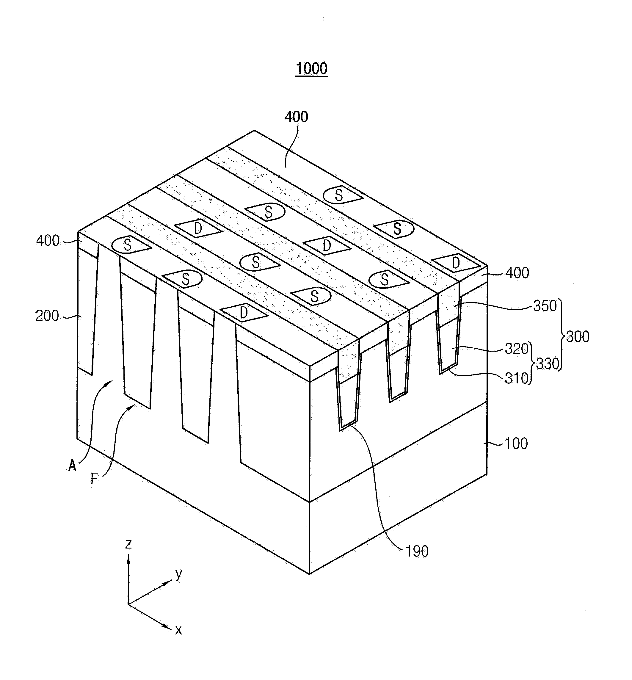
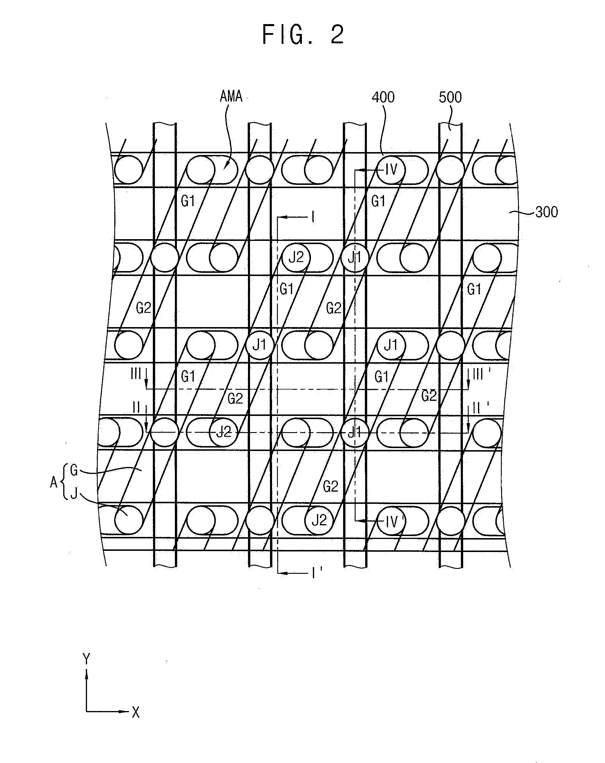
[0090]Example embodiments will now be described more fully with reference to the accompanying drawings. Embodiments, however, may be embodied in many different forms and should not be construed as being limited to the embodiments set forth herein. In the drawings, the thicknesses of layers and regions may be exaggerated for clarity.

[0091]It will be understood that when an element is referred to as being “on,”“connected to,” or “coupled to” to another component, it may be directly on, connected to, or coupled to the other component or intervening components may be present. In contrast, when a component is referred to as being “directly on,”“directly connected to,” or “directly coupled to” another component, there are no intervening components present. Other words used to describe the relationship between elements should be interpreted in a like fashion (e.g., “between” versus “directly between,”“adjacent” versus “directly adjacent,” etc.). However, the term “contact,” as used herein ...


PUM


Abstract

A semiconductor device includes a substrate having an active region defined by a device isolation layer and at least a gate trench linearly extending in a first direction to cross the active region, the active region having a gate area at a bottom of the gate trench and a junction area at a surface of the substrate. The device further may include a first conductive line filling the gate trench and extending in the first direction, the first conductive line having a buried gate structure on the gate area of the active region. The device also may include a junction including implanted dopants at the junction area of the active region, and a junction separator on the device isolation layer and defining the junction. The junction separator may be formed of an insulative material and have an etch resistance greater than that of the device isolation layer.

Description

CROSS-REFERENCE TO RELATED APPLICATIONS[0001]This application claims priority under 35 U.S.C §119 to Korean Patent Application No. 10-2015-0000787 filed on Jan. 5, 2015 in the Korean Intellectual Property Office, the disclosure of which is incorporated by reference herein in its entirety.BACKGROUND[0002]1. Field[0003]This disclosure relates to semiconductor devices and methods of manufacturing the same, and more particularly, to semiconductor devices having buried gate structures and methods of manufacturing the same.[0004]2. Description of the Related Art[0005]As the recent semiconductor devices tend to be downsized and high integrated, the pattern width has been reduced and the channel length has been shortened in a cell transistor. Thus, it has been getting more difficult to obtain a sufficient refresh time of memory devices due to the short channel effect.[0006]A recess channel array transistor (RCAT) has been introduced for obtaining a sufficient effective channel length. Howev...

Claims


Application Information

Patent Timeline
Patent Type & Authority Applications(United States)
IPC IPC(8): H01L27/108H01L21/761H01L21/311H01L29/423
CPCH01L27/10876H01L29/4236H01L27/1085H01L27/10891H01L21/31111H01L21/761H10B12/315H10B12/0335H10B12/053H10B12/488H01L29/66734H01L29/7843
Inventor YOON, CHAN-SICRYU, HO-INLEE, KI-SEOKCHO, CHANG-HYUN
Owner SAMSUNG ELECTRONICS CO LTD
Why Eureka
Try Eureka