Method and Apparatus for Creating and Placing a Micro Message

a micro-message and message technology, applied in electrical equipment, semiconductor devices, semiconductor/solid-state device details, etc., can solve the problems of high manufacturing cost, special equipment is required to fabricate, and the device size and structure of silicon wafer technology has become so small, so as to reduce the size of the transistor, the cost of building the fabs has risen, and the cost of manufacturing facilities is high

Inactive Publication Date: 2016-08-04
TRACKTHINGS
View PDF0 Cites 1 Cited by
  • Summary
  • Abstract
  • Description
  • Claims
  • Application Information

AI Technical Summary

Benefits of technology

[0006]As the size of the transistor decreases, the cost of building the fabs has risen to astronomical proportions causing the companies build these fabs these to join forces to share the expensive costs of creating factories to fabricate these silicon wafers that hold these atomically sized transistors. This high cost in manufacturing facilities translates to high cost to process a chip design

Problems solved by technology

The size and structure of the devices in the silicon wafer technology has become so small that special equipment is required to fabricate them.
As the size of the transistor decreases, the cost of building the fabs has risen to astronomical proportions causing the companie

Method used


Image

  • Method and Apparatus for Creating and Placing a Micro Message
  • Method and Apparatus for Creating and Placing a Micro Message
  • Method and Apparatus for Creating and Placing a Micro Message

Examples


Embodiment Construction

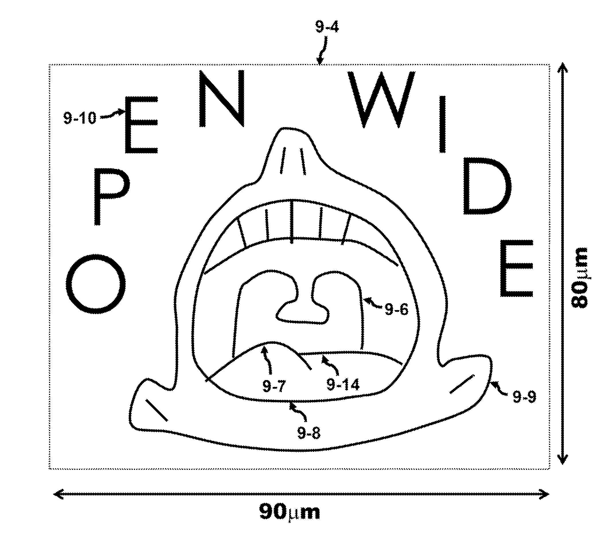
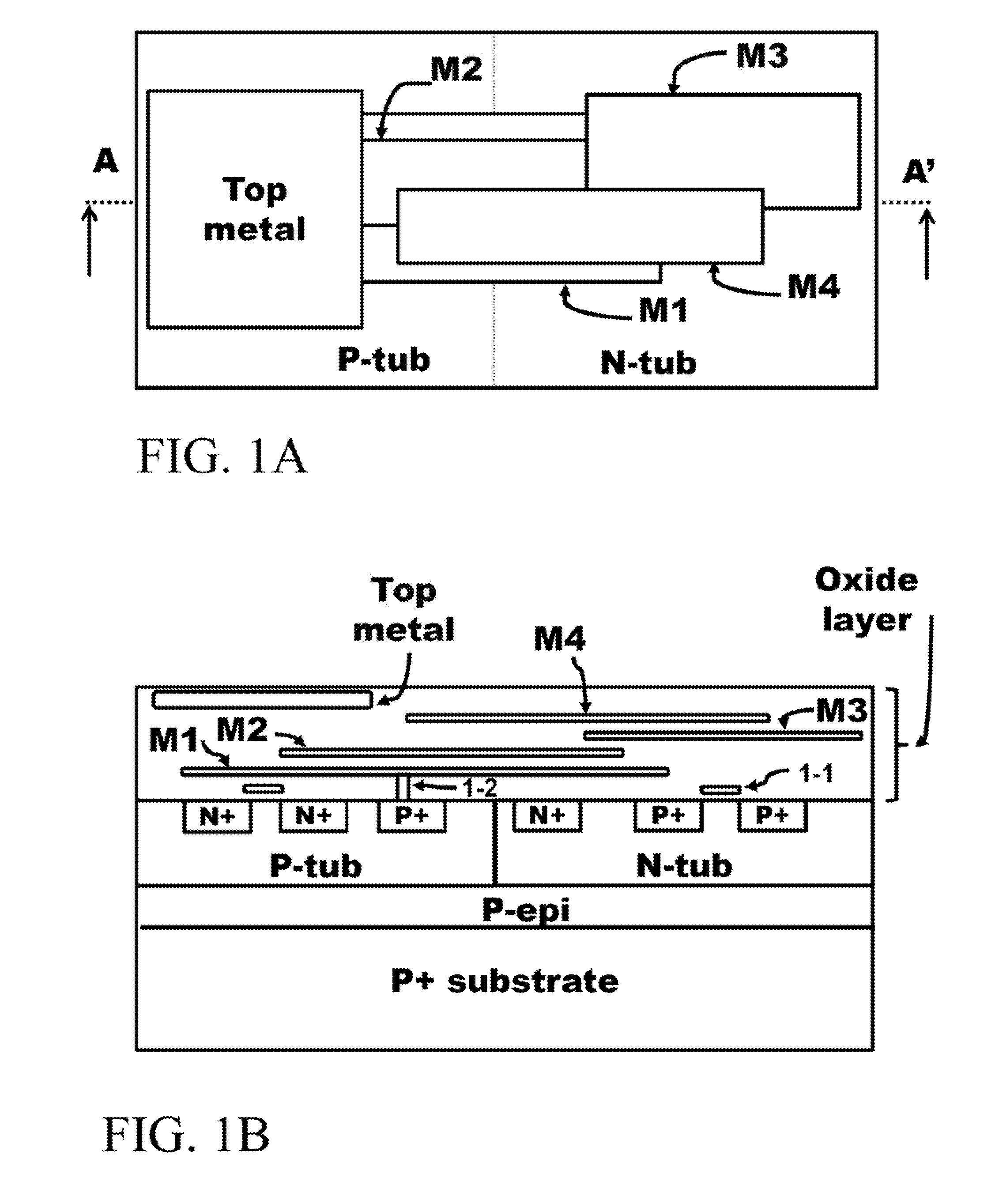
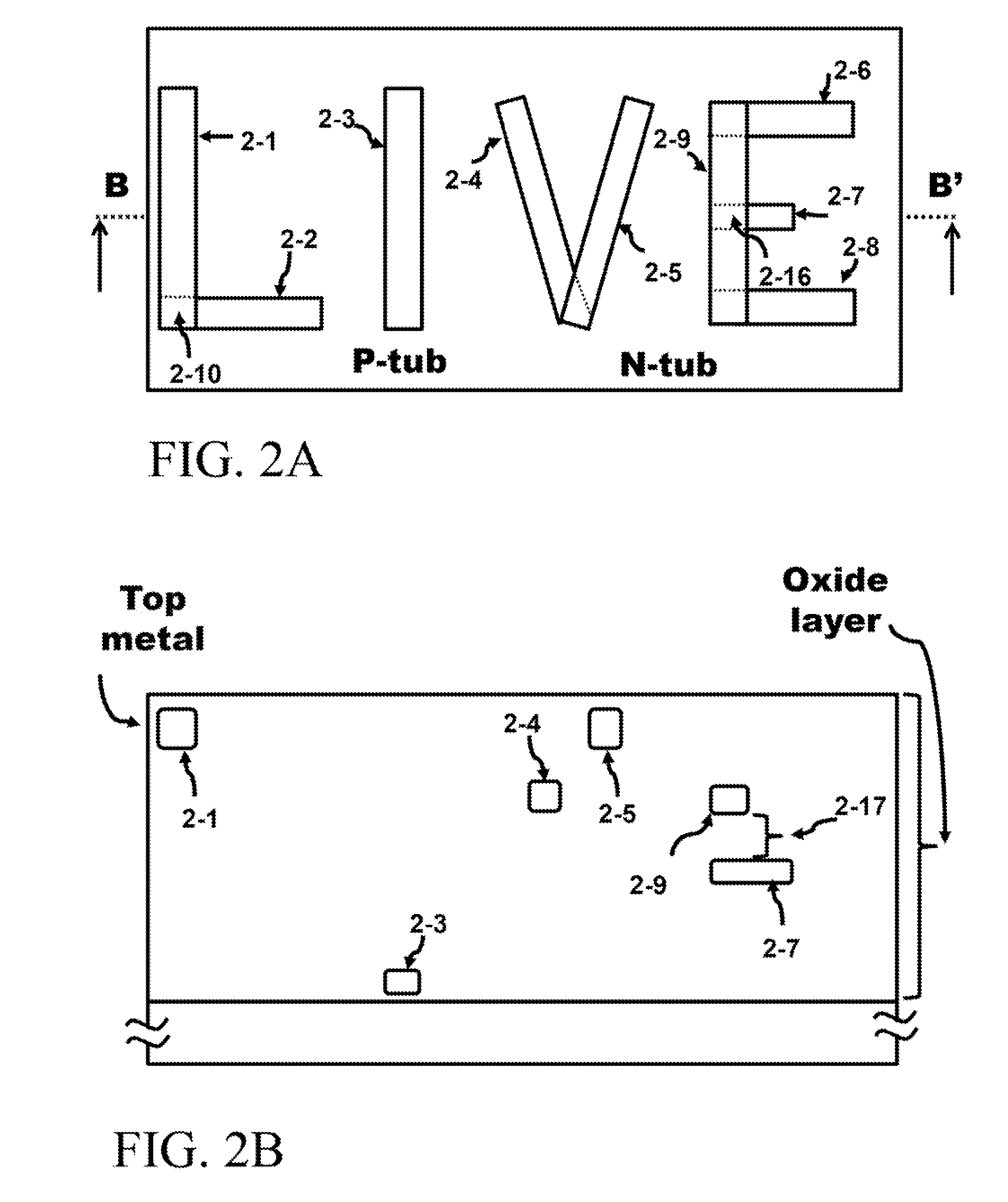
[0052]FIG. 1A illustrates a top view of a portion of a silicon wafer. The wafer has N-tub and P-tub doped regions in the substrate. The tubs typically have heavily doped p+ and n+ regions which are used to form tub ties, and define the source / drain regions of a transistor. If the starting substrate is p+, the N-tub can be patterned to form a conductor region. Furthermore, a heavily doped p+ region in an N-tub can be patterned to form another conductor region. Layers of oxide cover the substrate wherein between the layers of oxide, conductive traces are defined. These conductive traces could be formed from materials such as poly-silicon, aluminum, copper, etc. and can conduct electricity. The oxide, typically silicon dioxide but can be silicon nitride, is a non-conductor or insulator and does not conduct electricity. Two adjacent but not touching conductive traces are not electrically connected since an oxide separates the two conductive traces.

[0053]These conductive traces are usual...


PUM


Abstract

Silicon processing technology is used to generate an array of micro messages. These micro messages can contain at least one stick figure, or at least one word, or at least one stick figure and at least one word, or at least one stick figure and a grid mark, or at least one word and a grid mark, or at least one stick figure and at least one word and a grid mark. Grid marks are associated with the micro message and used to identify the X and Y Cartesian coordinates of the message. A plurality of conductive traces is used to form the micro messages. Each micro message can be completely encapsulated in silicon dioxide or at least one conductive trace can be connected to one of the tubs.

Description

CROSS REFERENCE TO RELATED APPLICATIONS[0001]Not applicable.BACKGROUND OF THE INVENTION[0002]Messages are one of the fundamental focuses of mankind. They tell stories, educate, remember, form building blocks of knowledge, and have propelled mankind on the forward journey into the future. Message come in a variety of forms: art on a wall, carved in stone, cast in steel, printed on paper, and voiced in words. Messages are created to leave a mark on the senses and thought. Some messages are ephemeral until the sound disappears, other messages last thousands of years like the hieroglyphs and the Rosetta stone. Words live in folklore; physical messages express history.[0003]Technology has helped to bring new methods of creating and storing messages possible. The telegraph, the telephone, radio, holography, electronic storage of sound, pictures, and video. Technology functioning for one purpose can be used to function as a medium to allow the creation and storage of messages in ways that ...

Claims


Application Information

Patent Timeline
IPC IPC(8): H01L23/544H01L23/528
CPCH01L2223/54406H01L23/544H01L2223/5442H01L2223/54426H01L2223/54433
Inventor GABARA, THADDEUS JOHN
Owner TRACKTHINGS
Why Eureka
Try Eureka