Semiconductor Device Having Shallow Trench Isolation Structure

a technology of isolation structure and semiconductor, which is applied in the direction of semiconductor devices, semiconductor/solid-state device details, electrical equipment, etc., can solve the problems of insufficient filling of narrow trenches of 30 nm or less in width, and the inferior performance of hdp-cvd in film burying performan

Active Publication Date: 2016-08-11
MICRON TECH INC
View PDF4 Cites 19 Cited by
  • Summary
  • Abstract
  • Description
  • Claims
  • Application Information

AI Technical Summary

Problems solved by technology

This is because that the HDP-CVD is so inferior in film-burying performance that narrow trenches of 30 nm or less in width cannot be filled sufficiently with a film by the HDP-CVD.

Method used


Image

  • Semiconductor Device Having Shallow Trench Isolation Structure
  • Semiconductor Device Having Shallow Trench Isolation Structure
  • Semiconductor Device Having Shallow Trench Isolation Structure

Examples


Embodiment Construction

[0013]Preferred embodiments of the present invention will now be described with reference to the accompanying drawings.

[0014]Experimental result knowledge obtained through experiments by the inventor will first be described, referring to FIGS. 6 and 7.

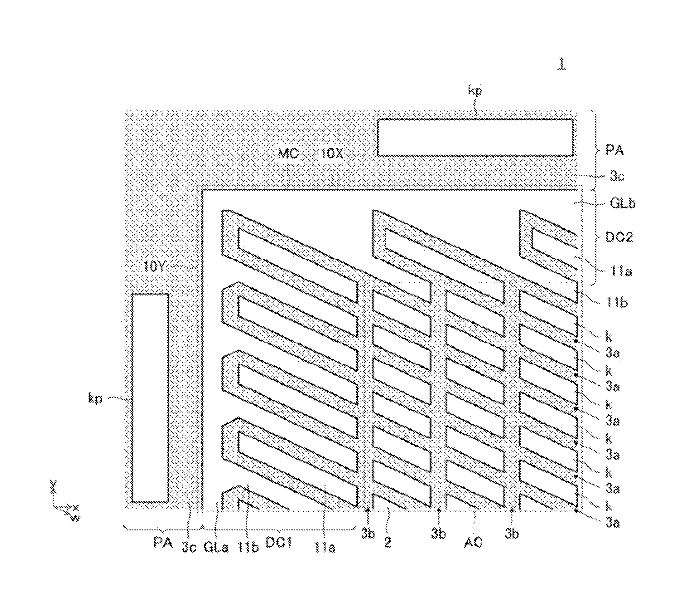
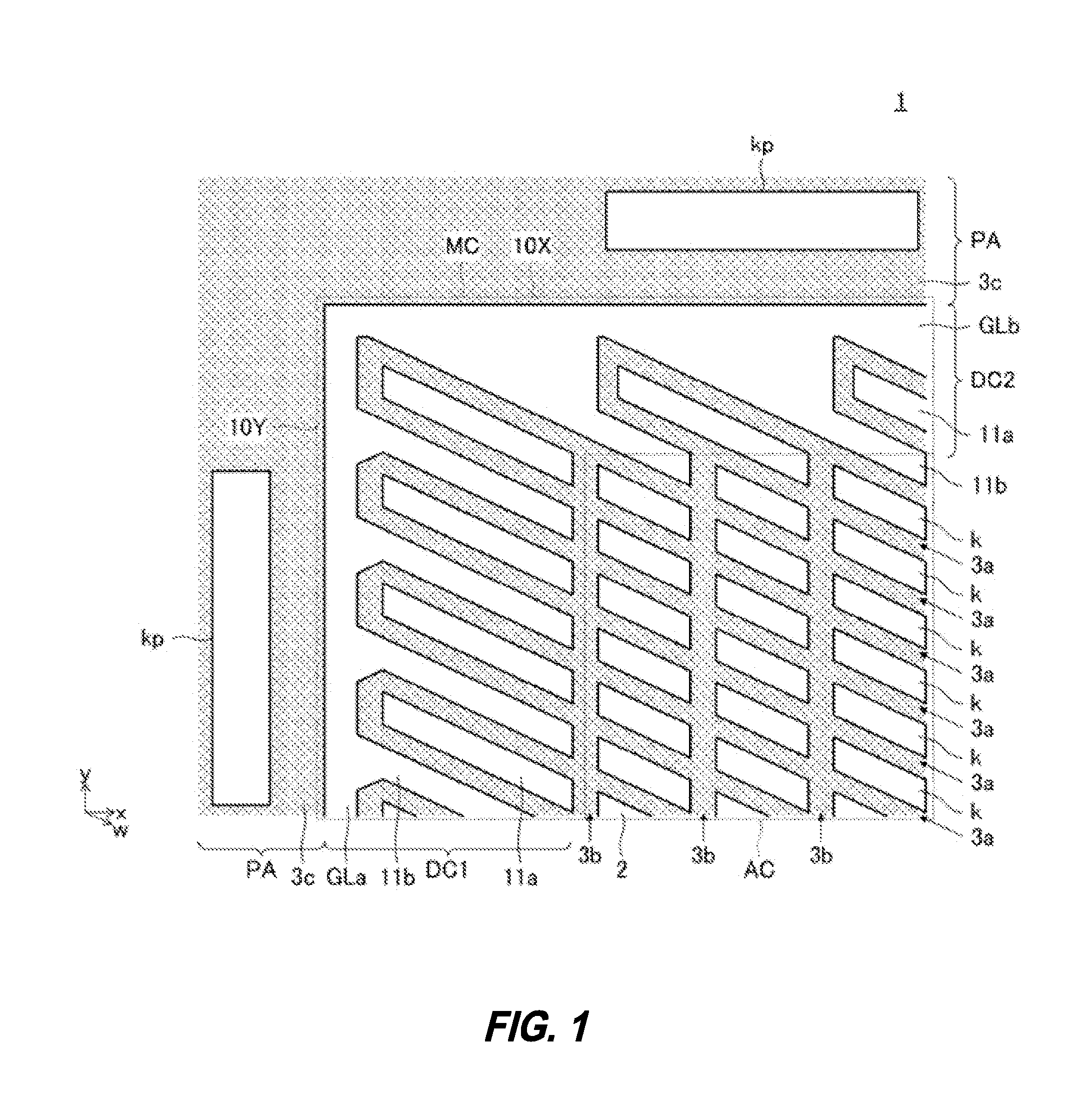
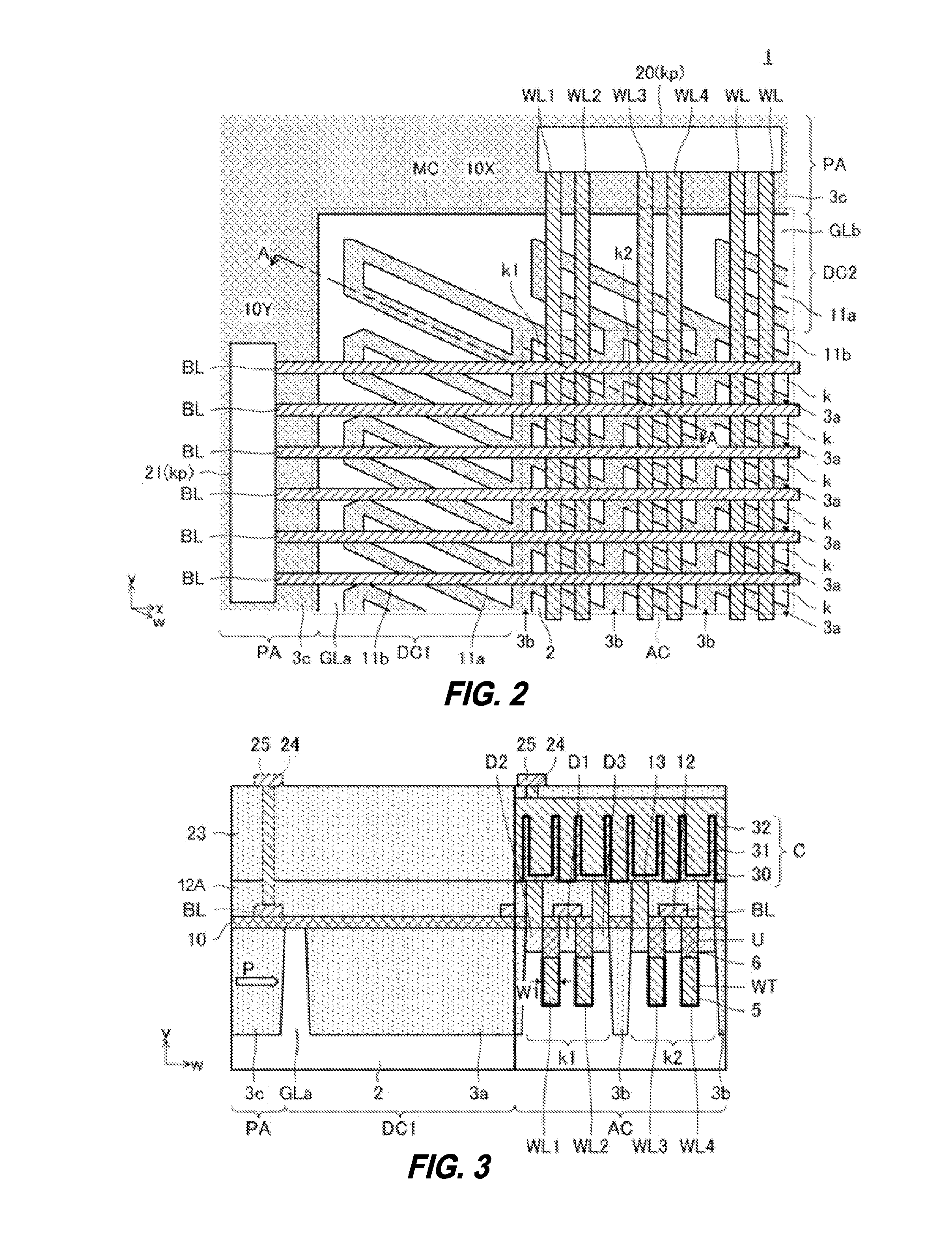
[0015]A semiconductor device 100 the inventor has experimented with is a DRAM, and is configured such that a memory cell area MC and a peripheral circuit area PA are defined on a main surface of a semiconductor substrate 2, as shown in FIGS. 6 and 7.

[0016]The memory cell area MC is a rectangular area having a first side 10Y extending in the y direction (first direction) and a second side 10X extending in the x direction (second direction) perpendicular to the y direction. The memory cell area MC includes a rectangular active cell area AC and a dummy cell area encircling the active cell area AC. The dummy cell area is composed of a first dummy cell area DC1 disposed along the first side 10Y and a second dummy cell area DC2 disposed alon...


PUM


Abstract

A semiconductor device is provided, which prevents a case where the widths of word lines become uneven because of a stress developing at the border between a memory cell area and a peripheral circuit area. The semiconductor device 1 has a semiconductor substrate 2 on which a memory cell area MC defined by a peripheral isolation region 3c. The memory cell area MC has multiple cell active regions k defined by multiple cell isolation regions 3a, 3b. Guard active regions GLa, GLb made of the semiconductor substrate are disposed in the border between the memory cell area MC and the peripheral isolation region 3c to separate the memory cell isolation regions 3a, 3b from the peripheral isolation region 3c.

Description

RELATED PATENT DATA[0001]This application is based upon and claims the benefit of priority from Japanese Patent Application No. 2015-024569 filed on Feb. 10, 2015, the disclosure of which is incorporated herein in its entirely by reference.TECHNICAL FIELD[0002]The present invention relates to a semiconductor device and particularly to a semiconductor device including a memory cell area and a peripheral circuit area disposed along the periphery of the memory cell area via an isolation region.BACKGROUND OF THE INVENTION[0003]A semiconductor device, such as DRAM (Dynamic Random Access Memory), includes a memory cell area and a peripheral circuit area disposed along the periphery of the memory cell area. Multiple active regions are arranged into matrix formation in the memory cell area, where the active regions are defined by isolation regions with a relatively small width. Multiple active regions are arranged also in the peripheral circuit area, where the active regions are defined by ...

Claims


Application Information

Patent Timeline
Patent Type & Authority Applications(United States)
IPC IPC(8): H01L29/06H01L23/528H01L27/108
CPCH01L29/0649H01L23/528H01L27/10897H01L21/762H10B12/315H10B12/50
Inventor TOMOYAMA, TSUYOSHI
Owner MICRON TECH INC
Why Eureka
Try Eureka