Light emitting diode

a technology of light-emitting diodes and electrode pads, which is applied in the direction of solid-state devices, electric devices, basic electric elements, etc., can solve the problems of current leakage, cracks in metal pads, and reduced so as to prevent the structure of electrode pads from cracking, reduce the stress on light-emitting diodes, and maintain the quality of light-emitting diodes

Inactive Publication Date: 2016-08-18
GENESIS PHOTONICS
View PDF3 Cites 13 Cited by
  • Summary
  • Abstract
  • Description
  • Claims
  • Application Information

AI Technical Summary

Benefits of technology

[0008]A light emitting diode of the present invention is mounted on a carrier substrate and includes a semiconductor epitaxial structure and at least one electrode pad structure. The semiconductor epitaxial structure is electrically connected to the carrier substrate through the at least one electrode pad structure. The electrode pad structure includes a eutectic layer, a blocking layer and an extension layer. The eutectic layer is adapted for eutectic bonding to the carrier substrate. The blocking layer is disposed between the eutectic layer and the semiconductor epitaxia

Problems solved by technology

However, during the eutectic bonding, the substrate is subjected to thermal expansion and contraction in the heating process, so stress is generated in the light emitt

Method used


Image

  • Light emitting diode
  • Light emitting diode
  • Light emitting diode

Examples


Embodiment Construction

[0038]Reference will now be made in detail to the present preferred embodiments of the invention, examples of which are illustrated in the accompanying drawings. Wherever possible, the same reference numbers are used in the drawings and the description to refer to the same or like parts.

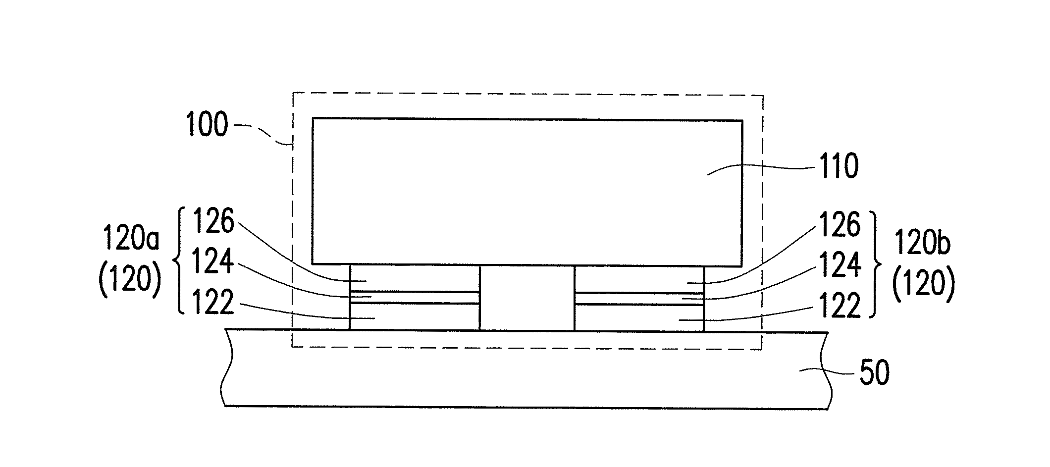
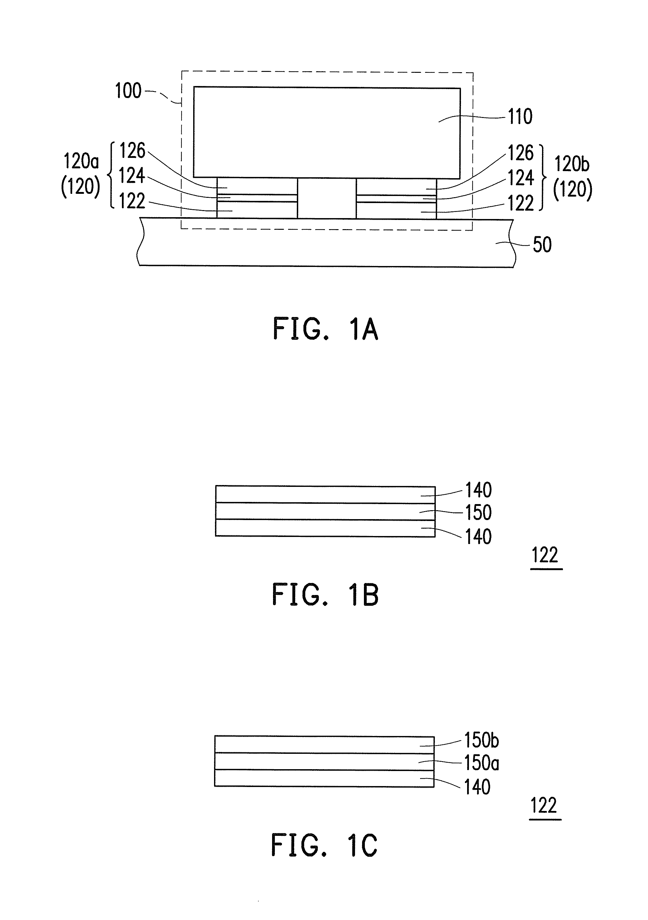
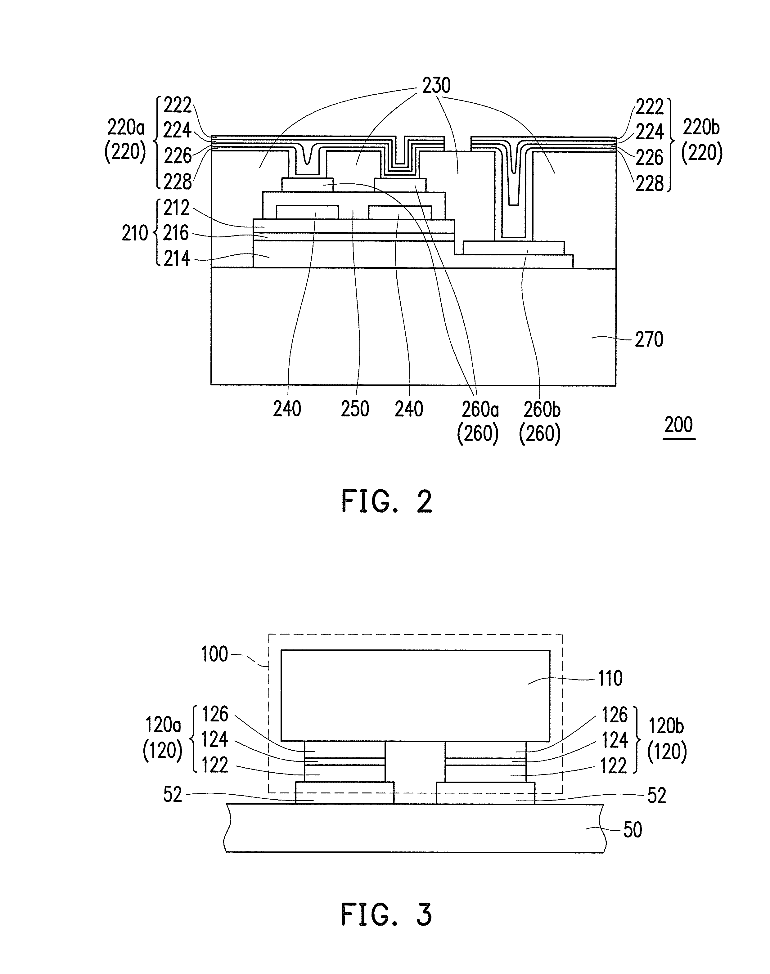
[0039]FIG. 1A is a schematic view of a light emitting diode mounted on a carrier substrate according to an embodiment of the present invention. Referring to FIG. 1A, a light emitting diode 100 includes a semiconductor epitaxial structure 110 and a plurality of electrode pad structures 120, and the light emitting diode 100 is mounted on a carrier substrate 50 through the electrode pad structures 120. The material of the semiconductor epitaxial structure 110 can be GaN, InGaN or another electroluminescent semiconductor material. However, the material of the semiconductor epitaxial structure 110 is not limited by the present invention. In this embodiment, the electrode pad structures 120 include a first...


PUM


Abstract

Provided is a light emitting diode (LED) mounted on a carrier substrate and including a semiconductor epitaxial structure and at least one electrode pad structure. The semiconductor epitaxial structure is electrically connected to the carrier substrate. The electrode pad structure includes a eutectic layer, a blocking layer and an extension layer. The eutectic layer is adapted for eutectic bonding to the carrier substrate. The blocking layer is between the eutectic layer and the semiconductor epitaxial structure. The blocking layer blocks the diffusion of the material of the eutectic layer in the eutectic bonding process. The extension layer is between the eutectic layer and the semiconductor epitaxial structure. The extension layer reduces the stress on the LED produced by thermal expansion and contraction of the substrate during the eutectic bonding process, so as to prevent the electrode pad structure from cracking, and maintain the quality of the LED.

Description

CROSS-REFERENCE TO RELATED APPLICATION[0001]The application claims the priority benefits of U.S. provisional application Ser. No. 62 / 116,923, filed on Feb. 17, 2015 and U.S. provisional application Ser. No. 62 / 148,761, filed on Apr. 17, 2015. The entirety of each of the above-mentioned patent applications is hereby incorporated by reference herein and made a part of this specification.BACKGROUND OF THE INVENTION[0002]1. Field of the Invention[0003]The present invention is related to a light emitting diode (LED).[0004]2. Description of Related Art[0005]A light emitting diode emits light by the recombination of electrons and holes therein when a current is applied to the semiconductor material thereof. As compared with a traditional light source, a light emitting diode has advantages of low power consumption, environment friendly, long service life and fast reaction speed, so the light emitting diode has been widely applied to the lighting field and the display field.[0006]Generally s...

Claims


Application Information

Patent Timeline
IPC IPC(8): H01L33/62
CPCH01L33/62H01L2933/0025H01L33/005H01L33/46H01L2224/16225H01L2224/32225H01L2224/48091H01L2224/48227H01L2224/48465H01L2224/73265H01L2924/00014H01L2924/00H01L33/50H01L33/44H01L33/10H01L33/40H01L33/36
Inventor HUANG, YI-RUCHUANG, TUNG-LINSHEN, CHIH-MINGHSU, SHENG-TSUNGHUANG, KUAN-CHIEHHUANG, JING-ENTING, SHAO-YING
Owner GENESIS PHOTONICS
Why Eureka
Try Eureka