Directional Heat Dissipation Assembly and Method

a heat dissipation assembly and directional technology, applied in the direction of semiconductor devices, semiconductor/solid-state device details, electrical apparatus, etc., can solve the problems of increasing the disparity in thermal conductivity, affecting the performance of the electrical system, and affecting the performance of the transistor, etc., to achieve the effect of increasing the disparity in thermal conductivities

Inactive Publication Date: 2016-09-01
WILKERSON JONATHAN RYAN
View PDF0 Cites 1 Cited by
  • Summary
  • Abstract
  • Description
  • Claims
  • Application Information

AI Technical Summary

Benefits of technology

[0013]In one embodiment, a thermal insulative layer encases a thermal conductive layer, with each layer having a substantially different thermal conductivity. The thermal insulative layer, in essence traps the heat, while the thermal conductive layer directionally transfers the heat towards the bottom or top surface of the transistor, and away from the sidewalls of the transistor. Thus, the diffusion of heat from the transistor is controlled by alternating layers of the thermal conductive layers and the thermal insulative layers, and / or by increasing the disparity in thermal conductivities between the thermal conductive layers and the thermal insulative layers.
[0046]Yet another objective is to diffuse heat from the transistor in a controlled manner by increasing the disparity in thermal conductivities between the thermal conductive layers and the thermal insulative layers.

Problems solved by technology

Electrical system performance and functionality of the transistor is often limited by heat dissipation in individual transistors or the net heat output of a group of transistors.
Regardless of low power design methodologies and power management techniques, fundamentally there will always be some amount of electrical power dissipated, which is turned into heat.
Stacked integrated circuits lack a readily accessible thermal dissipation channel, especially in thinned die, causing significantly higher temperature rises in circuits that can inhibit performance severely.
Limited options currently exist to address overheating of transistors.
At these levels, integrated circuits act as heaters in the facilities in which they are housed, which have to be cooled by HVAC or liquid cooling systems, often requiring significant energy to operate inside a facility.
The heat is spread as quickly as possible in virtually all cooling solutions to the local air in order to guarantee electrical performance, resulting in large electronics operating costs.
The problem with these systems is that they do not directionally guide the heat to a bottom and / or a top surface of a transistor.
Thus, an unaddressed need exists in the industry to address the aforementioned deficiencies and inadequacies.

Method used


Image

  • Directional Heat Dissipation Assembly and Method
  • Directional Heat Dissipation Assembly and Method
  • Directional Heat Dissipation Assembly and Method

Examples


second embodiment

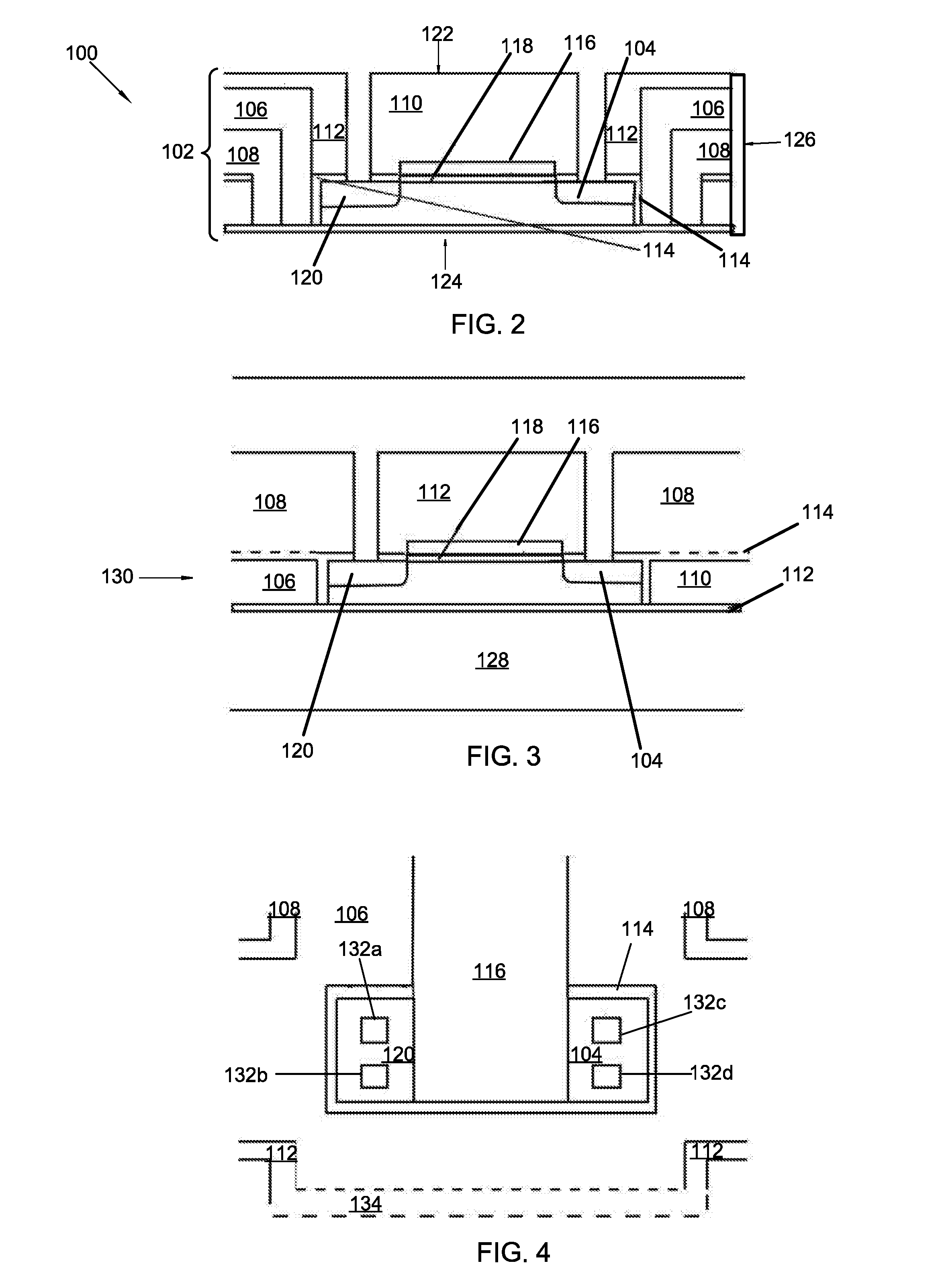
[0089]In a second embodiment, a structure of a transistor 130 with heat guiding structures for source, drain, and bulk regions including the conduction channel includes a directional heat guide member 102 composed of at least one layer or more of thermal conductivity layers encased in thermal insulative layers. The directional heat guide member 102 is connected to a heat source 120, drain, or bulk semiconductor 128 region, with connection to a heat source 120 or heat reservoir 104, i.e., drain region through a coupling barrier 114 that provides electrical isolation, and then connecting to the thermal conductor of the directional heat guide member 102.

[0090]In one exemplary use, the encasing thermal insulative layer 108 should be at least partially insulating the drain or source region. The directional heat guide member 102 should extend to a desired heat removal location, preferably, but not limited to, either a heat reservoir 104 or vertical directional heat guide, and finally coup...

third embodiment

[0091]In the present disclosure, a structure of a transistor 130 with a vertical heat guiding structure for source, drain, and channel regions includes: a transistor 130 surrounded along its perimeter by thermal insulator at least equal to the depth of the source and drain regions; an electrical insulator that is thermally conductive to a degree contacting the bottom of the transistor 130 or substrate directly under the transistor 130 within the thermally insulated region; and a directional heat guide which connects vertically through to the electrically insulating partially thermally conductive region.

fourth embodiment

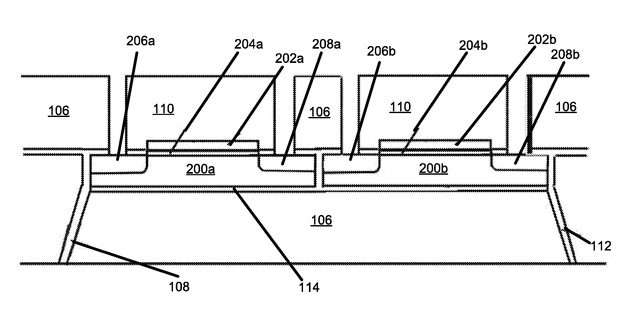
[0092]FIG. 7 illustrates a cross section view of a group of transistors coupled to a thermal guide for directional heat flow control. Thus, the directional heat guide member can encase a number of transistors where the outermost transistor define the thermal insulator of the heat guide. In the present disclosure shown in FIG. 7, a structure of a group of transistors 200a, 200b with vertical heat guiding members regions includes: a group of transistors 200a, 200b surrounded along their perimeter by thermal insulative layer at least equal to the depth of the source and drain regions; an electrical insulator that is thermally conductive to a degree contacting the bottom of the transistors or substrate directly under the transistors within the thermally insulated region; and a directional thermal guide member which connects vertically through to the electrically insulating partially thermally conductive region. Further including a group of gates 202a, 202b; a group of gate insulators 20...


PUM


Abstract

A directional heat diffusion assembly and method helps self-cool a transistor by forcing directional heat flow from a heat source, such as from a transistor, group of transistors, integrated circuit, or other integrated heat source, to a heat reservoir at a bottom surface and / or a top surface of the transistor, while also preventing heat flow towards the sidewall of the transistor. The directional heat flow occurs through a directional heat guide member that is comprised of alternating, layered arrangement of thermal insulative layers, and thermal conductive layers having varying thermal conductivities. In this manner, dissipation of heat through a directional heat guide member is controlled by either alternating the thermal insulative and conductive layers, or by increasing the differences between the thermal conductivities for the thermal insulative layers and thermal conductive layers

Description

CROSS REFERENCE OF RELATED APPLICATIONS[0001]This application claims the benefits of U.S. Nonprovisional application Ser. No. 14 / 280,543, filed May 16, 2014 and entitled FORCED DIRECTIONAL HEAT FLOW STRUCTURES AND METHODS, which Nonprovisional application is incorporated by reference herein in its entirety.FIELD OF THE INVENTION[0002]The present invention relates generally to a directional heat dissipation assembly and method. More so, a directional heat dissipation assembly provides a directional heat guide member that draws heat away from the coupled transistor through a top surface and a bottom surface of the transistor, while also inhibiting the transfer of heat towards the sidewall of the transistor with a layered arrangement of insulative and conductive materialBACKGROUND OF THE INVENTION[0003]Typically, a transistor is a semiconductor device used to amplify or switch electronic signals and electrical power. It is composed of semiconductor material with at least three terminal...

Claims


Application Information

Patent Timeline
Patent Type & Authority Applications(United States)
IPC IPC(8): H01L23/367H01L25/065H01L23/373H01L29/78H01L23/528
CPCH01L23/367H01L29/78H01L23/528H01L2225/06589H01L23/3735H01L25/0657H01L23/3731H01L2924/0002H01L2924/00
Inventor WILKERSON, JONATHAN RYAN
Owner WILKERSON JONATHAN RYAN
Why Eureka
Try Eureka