
Liquid Crystal Display Device and Method for Manufacturing the Same

a technology of liquid crystal display and sensing electrode, which is applied in the direction of instruments, computing, electric digital data processing, etc., can solve the problems of increased manufacturing cost, reduced device total thickness, and complicated manufacturing process

Active Publication Date: 2016-09-08
LG DISPLAY CO LTD
View PDF4 Cites 8 Cited by
  • Summary
  • Abstract
  • Description
  • Claims
  • Application Information

AI Technical Summary

Benefits of technology

This patent describes a method for manufacturing a LCD device that includes a pixel electrode and common electrode blocks. The common electrode blocks are made at a different layer from the pixel electrode and form an electric field to sense user touch. Sensing lines are electrically connected to the common electrode blocks and are insulated from the remaining common electrode blocks. The method includes sequentially forming layers and patterning sensing lines. A dummy area is also included to block ultraviolet rays. The technical effect of this invention is to improve the accuracy and efficiency of LCD device manufacturing.

Problems solved by technology

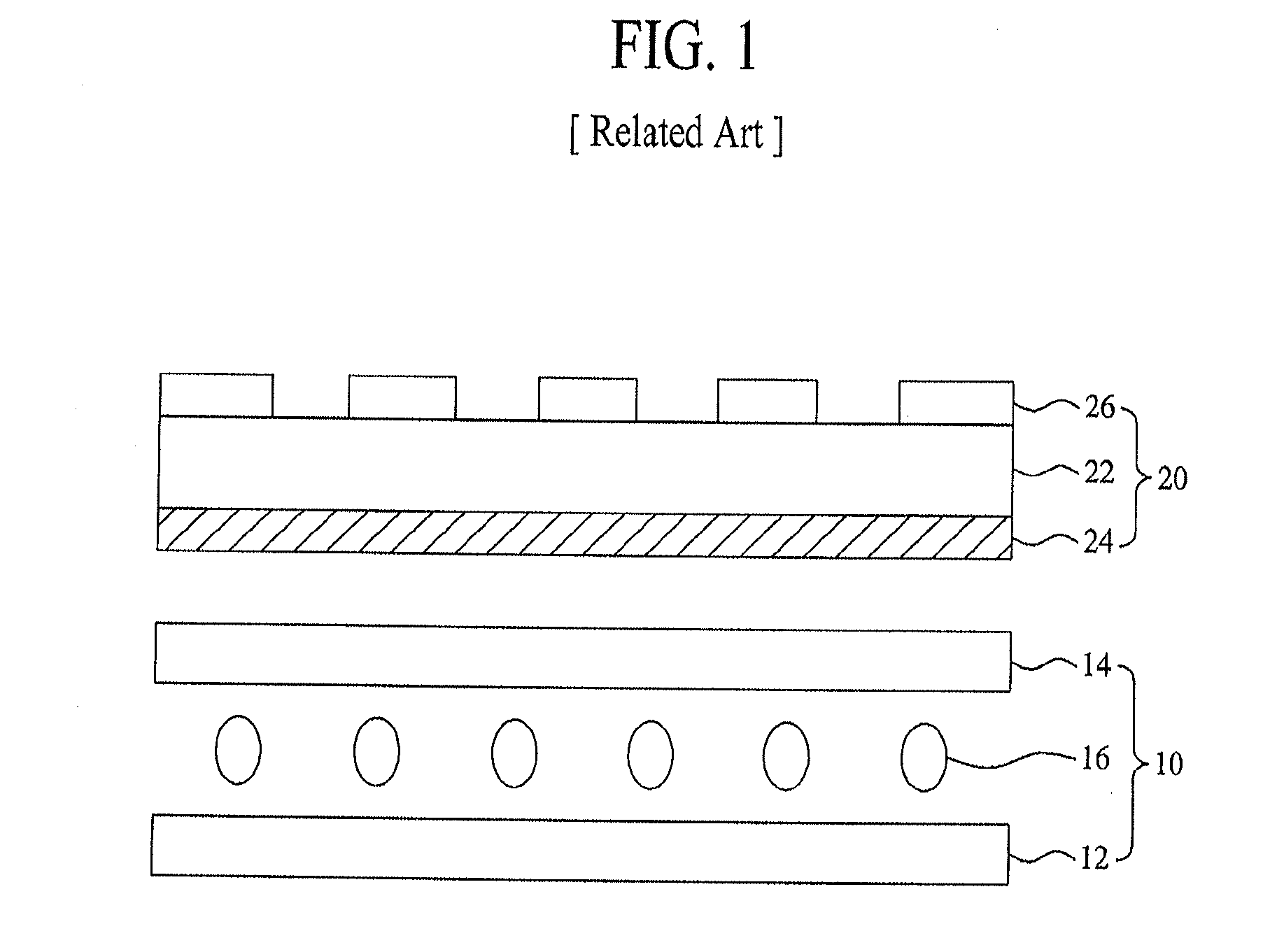
However, since the LCD device according to the related art is formed in a structure with the touch screen 20 additionally provided on the upper surface of the liquid crystal panel 10, it may cause disadvantages such as a decreased total thickness of the device, a complicated manufacturing process and an increased manufacturing cost.

Method used


Image

  • Liquid Crystal Display Device and Method for Manufacturing the Same
  • Liquid Crystal Display Device and Method for Manufacturing the Same
  • Liquid Crystal Display Device and Method for Manufacturing the Same

Examples


Embodiment Construction

[0033]Reference will now be made in detail to the exemplary embodiments of the present invention, examples of which are illustrated in the accompanying drawings. Wherever possible, the same reference numbers will be used throughout the drawings to refer to the same or like parts.

[0034]Hereinafter, a liquid crystal display (LCD) device according to the present invention and a method for manufacturing the same will be described with reference to the accompanying drawings.

[0035]On explanation about the embodiments of the present invention, if it is mentioned that a first structure is positioned ‘on or above’ or ‘under or below’ a second structure, it should be understood that the first and structures are brought into contact with each other, or a third structure is interposed between the first and second structures.

Liquid Crystal Display (LCD) Device

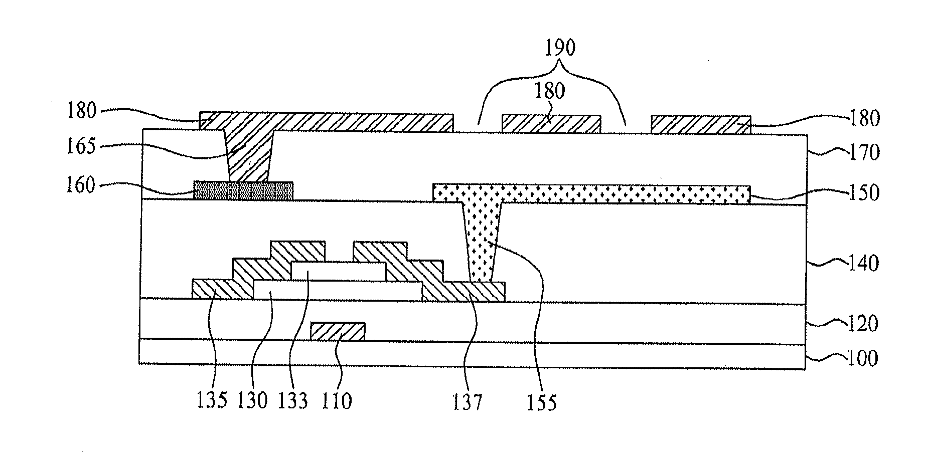
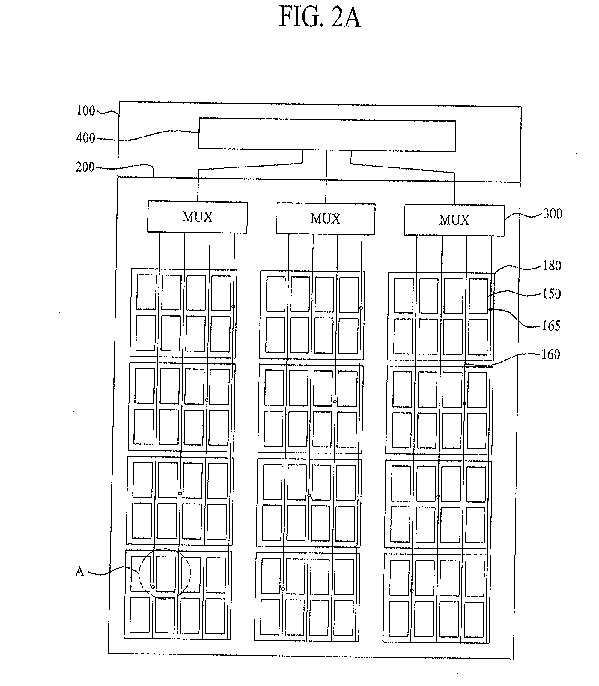
[0036]FIG. 2A is a plane view of a lower substrate for an LCD device according to one embodiment of the present invention, FIG. 2B shows a...


PUM

PropertyMeasurementUnit
resistanceaaaaaaaaaa
electricalaaaaaaaaaa
electric fieldaaaaaaaaaa

Abstract

Disclosed is an LCD device which realizes decreased thickness, simplified process, and decreased cost by using a common electrode for formation of electric field to drive liquid crystal as a sensing electrode, and removing a touch screen from an upper surface of the liquid crystal panel, the LCD device comprising gate and data lines crossing each other to define plural pixels on a lower substrate; a pixel electrode in each of the plural pixels; plural common electrode blocks patterned at the different layer from the pixel electrode, wherein the common electrode blocks, together with the pixel electrode, forms an electric field, and senses a user's touch; and plural sensing lines electrically connected with the common electrode blocks, wherein, if the sensing line is electrically connected with one of the common electrode blocks, the sensing line is insulated from the remaining common electrode blocks.

Description

CROSS REFERENCE TO RELATED APPLICATIONS[0001]This application claims the benefit of the Korean Patent Application No. 10-2011-0140094 filed on Dec. 22, 2011, which is hereby incorporated by reference as if fully set forth herein.BACKGROUND[0002]1. Field of the Disclosure[0003]The present disclosure relates to a liquid crystal display (LCD) device, and more particularly, to a liquid crystal display (LCD) device with a sensing electrode for sensing a user's touch.[0004]2. Discussion of the Related Art[0005]Owing to advantages such as good portability and low power consumption by low operating voltage, a liquid crystal display (LCD) device is widely used in various fields of notebook computer, monitor, spacecraft, aircraft, etc.[0006]The LCD device includes a lower substrate, an upper substrate, and a liquid crystal layer formed between the lower and upper substrates. According to whether or not an electric field is applied, light transmittance is controlled by alignment of the liquid ...

Claims


Application Information

Patent Timeline
Patent Type & Authority Applications(United States)
IPC IPC(8): G02F1/1333G02F1/1343G06F3/047G02F1/1368G06F3/041G02F1/1335G02F1/1362
CPCG02F1/13338G02F1/133345G02F1/133514G02F1/134309G02F1/13439G02F2001/136295G02F1/1368G06F3/0412G06F3/047G02F2001/133302G06F2203/04103G02F1/136286G06F3/044G02F1/134372G06F3/0443G06F2203/04111G02F1/133302G02F1/136295G06F3/041
Inventor SHIN, HEESUNLEE, SEOK WOOYU, JAE SUNGKIM, JU HANLEE, SUN JUNGSONG, IN HYUK
Owner LG DISPLAY CO LTD
Learn More