
Memory self-testing device and method thereof

a self-testing device and memory technology, applied in the field of memory self-testing devices and methods, can solve the problems of excessively long activation time and achieve the effect of reducing test tim

Active Publication Date: 2016-09-08
XUESHAN TECH INC
View PDF0 Cites 3 Cited by
  • Summary
  • Abstract
  • Description
  • Claims
  • Application Information

AI Technical Summary

Benefits of technology

The present invention is a device and method that simultaneously tests multiple memory control units using a single testing device. This reduces testing time, making the testing process faster without significantly increasing circuit costs.

Problems solved by technology

Such time-consuming process results in an excessively long activation time.

Method used


Image

  • Memory self-testing device and method thereof
  • Memory self-testing device and method thereof
  • Memory self-testing device and method thereof

Examples


Embodiment Construction

[0024]Technical terms of the application are based on the general definition in the technical field of the application. If the application describes or explains one or some terms, definitions of the terms are based on the description or explanation of the application.

[0025]The disclosure of the present invention includes a memory self-testing device and method capable of simultaneously testing a plurality of memory control units. In possible implementation, one person skilled in the art can choose equivalent elements or steps to achieve the present invention according to the disclosure of the application. That is, the implementation of the present invention is not limited to the embodiments below.

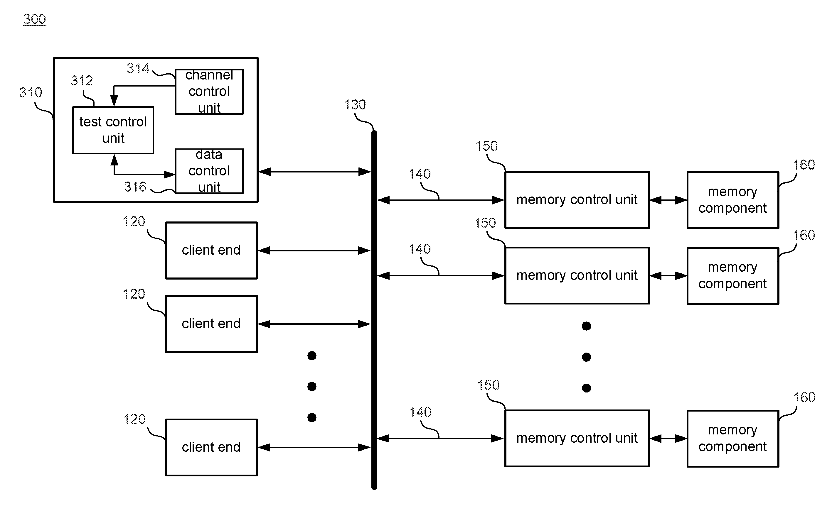
[0026]FIG. 3 shows a block diagram of a circuit system including a multi-channel memory self-testing device according to an embodiment of the present invention. A circuit system 300 tests channels 140 and memory control units 150 by a multi-channel memory self-testing device 310. Clocks and...


PUM


Abstract

A memory self-testing device for testing a plurality of memory control units includes: a test control unit, coupled to the memory control units, generating a plurality of access request signals and a plurality of sets of data; a channel control unit, coupled to the test control unit and the memory control units, determining a leading feedback signal among a plurality of feedback signals; and a data control unit, coupled to the test control unit and the memory control units, storing the sets of data, and transmitting the sets of data to the memory control units according to a plurality of read / write signals. The feedback signals and the read / write signals are generated by the memory control units in response to the access request signals. The test control units generate the sets of data according to the leading feedback signal.

Description

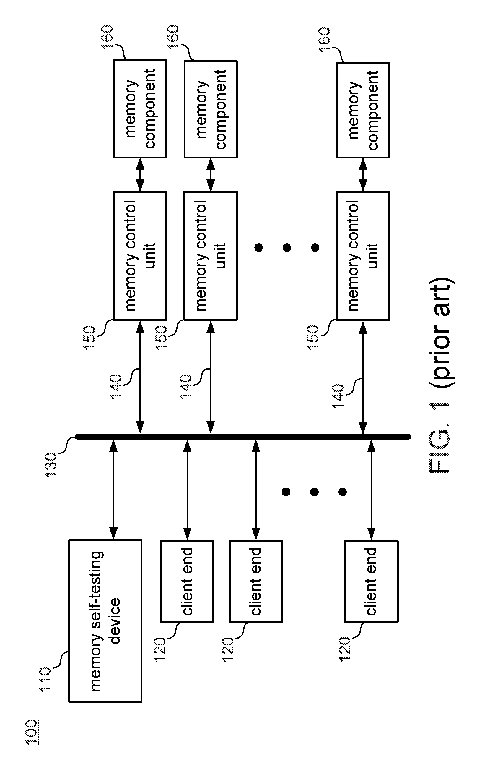
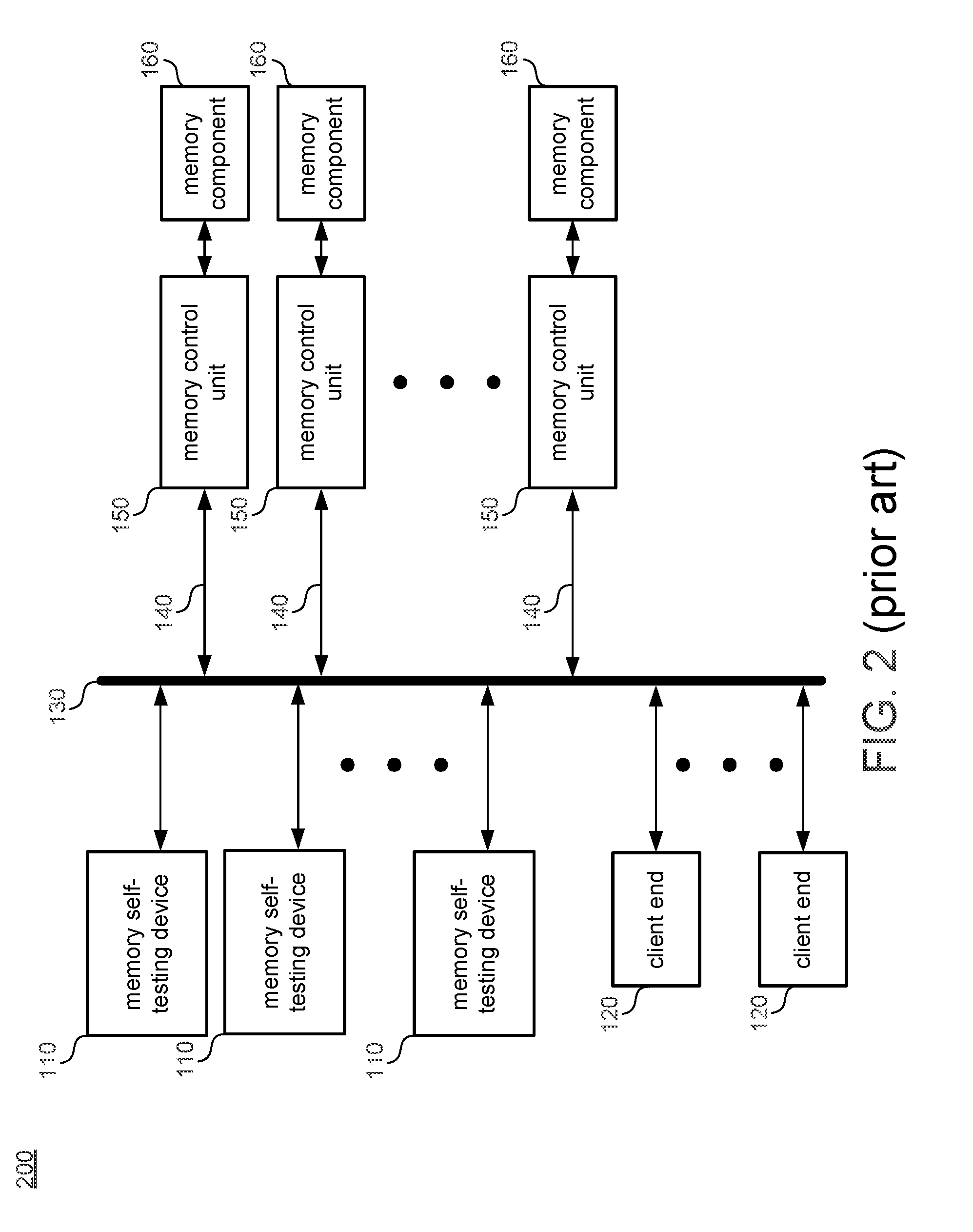
[0001]This application claims the benefit of Taiwan application Serial No. 104106618, filed Mar. 3, 2015, the subject matter of which is incorporated herein by reference.BACKGROUND OF THE INVENTION[0002]1. Field of the Invention[0003]The invention relates in general to a memory self-testing device and method, and more particularly to a memory self-testing device and method for testing whether channels and memory control units of a memory are functional.[0004]2. Description of the Related Art[0005]FIG. 1 shows a block diagram of a conventional circuit system including a memory self-testing device. For example, the circuit system 100 is a partial circuit of a digital television system, and includes a memory self-testing device 110, a plurality of client ends 120, a bus 130, a plurality of channels 140, a plurality of memory control units (e.g., memory interface units, MIUs) 150, and a plurality of memory components 160. Each client end 120 is a function module of the television system...

Claims


Application Information

Patent Timeline
IPC IPC(8): G11C29/04G11C11/417
CPCG11C11/417G11C29/04G11C29/16G06F11/2094G06F11/27G11C29/025G11C29/52G11C2029/0401
Inventor CHEN, CHUNG-CHINGLIN, CHEN-NANLO, YI-HAO
Owner XUESHAN TECH INC
Learn More