Photonic integrated circuit
a technology of integrated circuits and photonics, applied in the field of photonic integrated circuits, can solve the problems of reducing the electric resistance affecting the signal transmission speed of the semiconductor integrated circuit, and affecting the speed of signal transmission between the semiconductor integrated circuits
- Summary
- Abstract
- Description
- Claims
- Application Information
AI Technical Summary
Benefits of technology
Problems solved by technology
Method used
Image

Examples
first embodiment
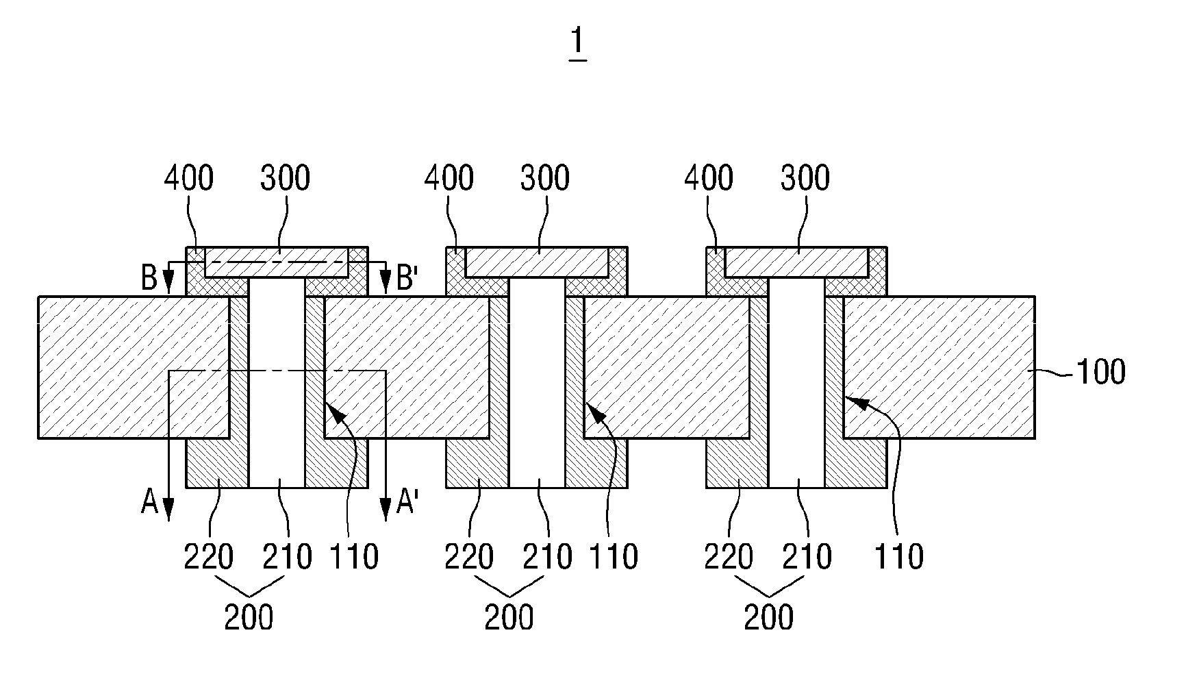
[0041]A photonic integrated circuit will now be described with reference to FIGS. 1 to 3.
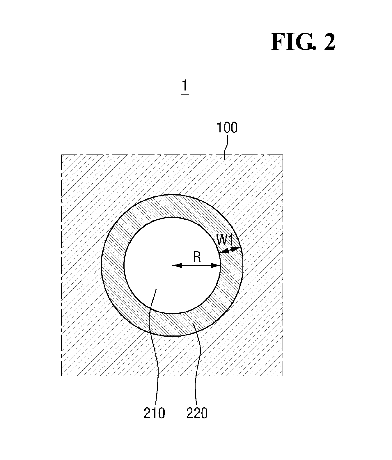
[0042]FIG. 1 is a cross-sectional view for describing the photonic integrated circuit according to the first embodiment. FIG. 2 is a cross-sectional view taken along the line A-A′ of FIG. 1. FIG. 3 is a top view taken along the line B-B′ of FIG. 1.
[0043]Referring to FIG. 1, a photonic integrated circuit 1 according to the first embodiment includes a substrate 100, transmission wire 200, a converter 300 and an electrical terminal 400.
[0044]The substrate 100 may include any substrate on which a photonic integrated circuit may be formed. For example, the substrate 100 may include a rigid substrate such as a silicon substrate, a silicon on insulator (SOI) substrate, a gallium arsenide substrate, a silicon germanium substrate, a ceramic substrate, a quartz substrate or a glass substrate for a display, or a flexible plastic substrate such as a polyimide substrate, a polyester substrate, a polycarbona...
third embodiment
[0072]Referring to FIG. 5, an electrical transmission film 222 of a photonic integrated circuit 3 may not completely surround and thus expose a part of outer surfaces of the optical transmission line 210 and the reflective layer 230. Since the reflective layer 230 of the optical transmission line 210 exists, the electrical transmission film 222 does not need to reflect the optical signal in the optical transmission line 210, and thus it is possible to form the electrical transmission film 222 such that the electrical transmission film 222 does not completely surround the outer surfaces of the optical transmission line 210 and the reflective layer 230.
[0073]Thus, the electrical transmission film 222 of the photonic integrated circuit 3 according to the third embodiment may contact only a part of the outer surface of the reflective layer 230 and expose a part of the outer surface of the reflective layer 230. Accordingly, a design in which a part of the electrical transmission film 22...
fourth embodiment
[0077]Referring to FIG. 6, an electrical transmission film 223 of a photonic integrated circuit 4 may include multiple sub electrical transmission films 223 and an insulation film 240.
[0078]The sub electrical transmission films 223 may include a first sub electrical transmission film 223a and a second sub electrical transmission film 223b. The sub electrical transmission films 223 may be electrically insulated from each other. That is, each sub electrical transmission film 223 may transmit different electrical signals.
[0079]The insulation film 240 may be formed between the sub electrical transmission films 223. Although the sub electrical transmission films 223 are depicted as two in FIG. 6, the number of the sub electrical transmission films 223 is not restricted as long as the number more than one. Multiple insulation films 240 may be present. The insulation film 240 may electrically insulate the sub electrical transmission films 223 from each other. That is, the insulation film ...
PUM
 Abstract
Description
Claims
Application Information
 - R&D
- Intellectual Property
- Life Sciences
- Materials
- Tech Scout
- Unparalleled Data Quality
- Higher Quality Content
- 60% Fewer Hallucinations
Browse by: Latest US Patents, China's latest patents, Technical Efficacy Thesaurus, Application Domain, Technology Topic, Popular Technical Reports.
© 2025 PatSnap. All rights reserved.Legal|Privacy policy|Modern Slavery Act Transparency Statement|Sitemap|About US| Contact US: help@patsnap.com