
Multi-chip touch architecture for scalability

a touch controller and multi-chip technology, applied in computing, instruments, electric digital data processing, etc., can solve the problems of unsuitability of existing touch controller architectures for scalability, and achieve the effects of improving processing speed, minimizing data transfer, and improving processing speed

Active Publication Date: 2016-09-15
APPLE INC
View PDF10 Cites 54 Cited by
  • Summary
  • Abstract
  • Description
  • Claims
  • Application Information

AI Technical Summary

Benefits of technology

The patent is about a touch controller that can process touch data from a touch sensor panel. The touch controller includes a memory and processing circuits to analyze the touch data and identify touch events. The processing circuits can use hardware accelerators to speed up the processing process. The main technical effect of this invention is to enable faster and more parallel processing of touch images by multiple touch controllers, improving the overall performance and accuracy of touch sensing.

Problems solved by technology

As the sizes of touch screens vary in size and across device platforms, existing touch controller architectures can be unsuitable for scalability.

Method used


Image

  • Multi-chip touch architecture for scalability
  • Multi-chip touch architecture for scalability
  • Multi-chip touch architecture for scalability

Examples


Embodiment Construction

[0031]In the following description of examples, reference is made to the accompanying drawings which form a part hereof, and in which it is shown by way of illustration specific examples that can be practiced. It is to be understood that other examples can be used and structural changes can be made without departing from the scope of the disclosed examples.

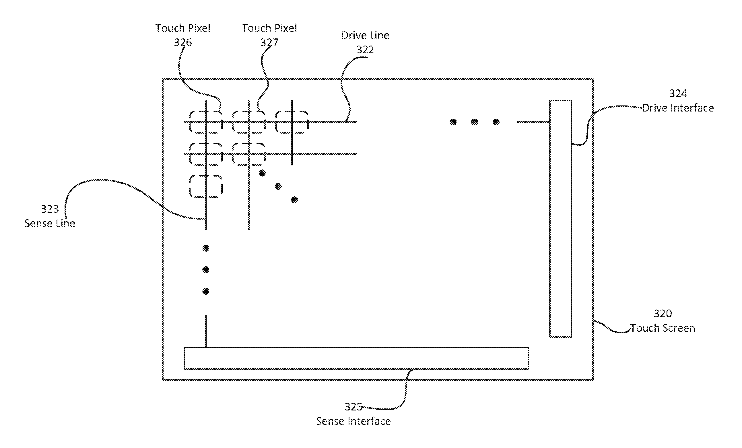
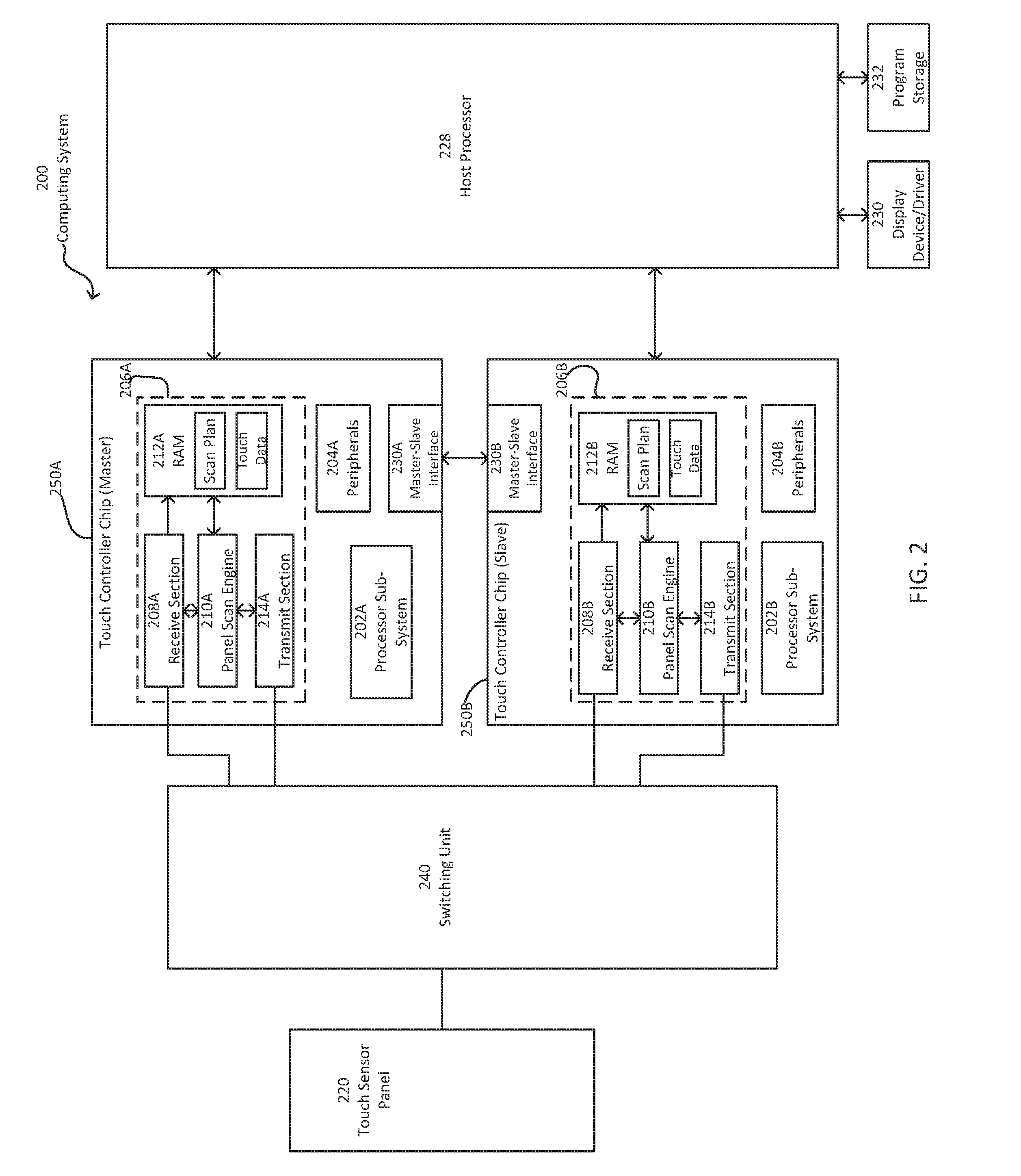
[0032]This relates to multi-chip touch architecture for scalability. A touch-sensitive device can include a touch sensor panel, one or more touch controller application specific integrated circuits (ASICs), and one or more switching circuits coupled between the one or more touch controller ASICs and the touch sensor panel. Each touch controller ASIC can be coupled to one or more switching circuits. The number of touch controller ASICs and switching circuits can be scaled based on the size of the touch sensor panel.

[0033]The touch controller ASICs can include an interface including one or more ports to communicate with one another ...


PUM


Abstract

A multi-chip touch architecture for scalability can include one or more touch controller application specific integrated circuits (ASICs), and one or more switching circuits coupled between the one or more touch controller ASICs and the touch sensor panel. The number of touch controller ASICs and switching circuits can be scaled based on the size of the touch sensor panel. The touch controller ASICs can include an interface for data transfer between the touch controller ASICs to allow for parallel processing of an image of touch by more than one touch controller ASIC. The touch controller ASIC can also include a memory directly accessible by more than one processing circuit (e.g., hardware accelerators), and circuitry to dynamically adjust the coupling between portions (e.g., banks) of memory and inputs of the one or more processing circuits to minimize data transfer and improve processing speeds.

Description

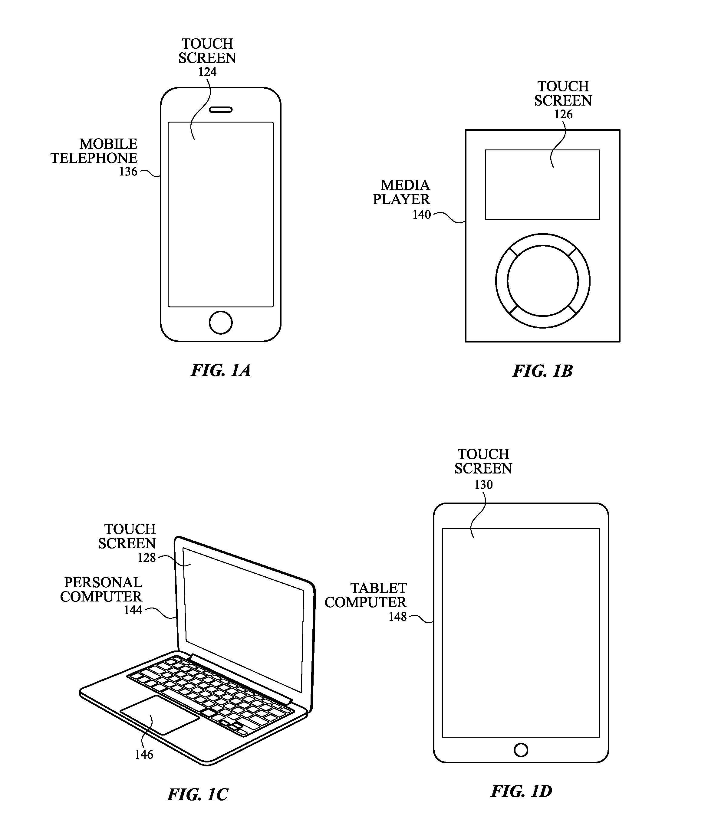
CROSS REFERENCE TO RELATED APPLICATIONS[0001]This application claims the benefit of U.S. Provisional Application No. 62 / 131,242 filed on Mar. 10, 2015, the entire disclosure of which is herein incorporated by reference for all purposes.FIELD OF THE DISCLOSURE[0002]This relates generally to touch-sensitive devices, and more particularly, to multiprocessor touch controller architectures.BACKGROUND OF THE DISCLOSURE[0003]Many types of input devices are presently available for performing operations in a computing system, such as buttons or keys, mice, trackballs, trackpads, joysticks, touch sensor panels, touch screens and the like. Touch screens, in particular, are becoming increasingly popular because of their ease and versatility of operation as well as their declining price. Touch screens can include a touch sensor panel, which can be a clear panel with a touch-sensitive surface, and a display device such as a liquid crystal display (LCD) that can be positioned partially or fully be...

Claims


Application Information

Patent Timeline
Patent Type & Authority Applications(United States)
IPC IPC(8): G06F3/044
CPCG06F3/044G06F3/0416G06F3/04184G06F3/04166
Inventor SHAHPARNIA, SHAHROOZPANT, VIVEKKRAH, CHRISTOPH H.
Owner APPLE INC
Learn More